Keywords
MS and MPS structures; Passivation effect; Surface states; Negative capacitance
Introduction
Recently, many of experimental researches and studies for the metal-polymer-semiconductor (MPS) type structures in order to replacing the traditional metal-semiconductor (MS) structures with and without insulation interfacial layer such as SiO2 or SnO2 [1-7]. In general, pure polymer usually is a poor conductivity material, but its conductivity can be increased by using doping with a metal at appropriate rates [8-11]. Therefore, polymer interfacial layers attract considerable attention in the electronic and optoelectronic devices due to their easy device fabrication, flexibility, low cost, suitability.
There are different kinds of polymers/organics among of them is poly (vinyl alcohol) (PVA) that has a semi-crystalline structure and high water-solubility, nontoxic, crystallinity with wide range, good charge/energy storage capacity and high dielectric strength properties [12-15].
In addition, PVA is from hydroxyl group; therefore it can be reacts easily with other organic and inorganic compounds. Therefore, in very recently, it is believed that MPS structure is considered one of the most promising candidates in the future semiconductor technology instead of classic/conventional MS, MOS and MIS type structures [8-15].
At the same time, silicon carbide (SiC) represents a very important semiconductor among many kinds of semiconductor crystals with wide band-gap (Eg) [16]. Furthermore, SiC is 3 times wider Eg (=3.2 eV) and 10 times higher critical electric field (E=2.2 × 10⁶ V/cm) when compared conventional Si semiconductor [17].
It is clear that the electrical properties of MS structure with exist of insulator or organic interfacial layer and without it usually not only depend on the metal and interfacial layer used, but depend strongly on the surface properties, doping concentration level of semiconductor, barrier form at the interface between metal and semiconductor, series and shunt resistances of the device (Rs and Rsh) and applied bias voltage across the junction [18-26]. Especially, high-dielectric interlayer can cause the leakage reverse current, n, Rs and Nss, and increase the BH, intercept voltage (Vi or Vo) and Rsh [27]. Zinc (Zn), Cobalt (Co) and nickel (Ni) were used as doped materials due to low cost, abundant raw material and heat cycling. The other more important feature of the SiC is the ability to form SiO2 as a native insulator/oxide layer. There are still a number of factors which are limiting the device performance such as the formation of back Ohmic contact with low resistivity and high-temperature stable Schottky/rectifier contacts. Both Zn and SiC have also the same wurtzite crystal symmetry and relatively higher lattice mismatch (5%). Although there are various “poly-types” SiC, but the most preferred among is 4H-SiC due to its superior physical properties through owing double electron mobility as compare with 6H-SiC at a given dopant density and the availability of high-quality epitaxial wafers [27-30].
In this study, the experimental result give us a good indicate about how is the effect of modified PVA interfacial layer doped by Zn nanoparticles on electrical properties and conduction/transport mechanism, therefore, after we fabricate Au/n-SiC (MS) and Au/ (Zn-PVA)/n-4H SiC (MPS) structures, we calculate and investigate the main electrical parameters for both structures to compare between them by using the forward and reverse bias I-V, C-V and G/ω-V measurements at room temperature. The interface state energy distribution profiles of Nss were obtained from the forward bias I-V data for two type structures by taking into account voltage dependent BH and ideality factor. As a results of comparison between the two structures, it was found that the modified PVA interfacial layer doped by Zn nanoparticles leads to a decrease in the values Nss, Rs, leakage current and increase in shunt resistance (Rsh) and RR.
Experimental Details
Au/n-4H SiC (MS) and Au/Zn-PVA/n-SiC (MPS) with modified PVA interfacial layer doped by Zn nanoparticles structures were fabricated by using two same quarter n-type 4H-SiC (0001) wafer with the following properties: donor concentration atoms (Nd) about 7.07 × 1017 cm-3, rectifying contact area 0.0314 cm2 and thickness about 250 μm. for fabrication process, firstly, n-type 4H-SiC wafer was dipped in organic solution of ammonium peroxide solution for 10 minutes to remove any oxide thin layer that could be cover it, and then etched in a sequence of acidic solution H2O+HCl by using ultrasonic bath and then quenched in de-ionized water (DI) with 18 MΩ.cm resistivity for 10 minutes. Preceding each cleaning step, the wafer was rinsed thoroughly in DI water. Finally, n-4H SiC wafer dried in the high-pure dry nitrogen (N2) gas to prevent any oxidation of the wafer and then high purity (99.999%) Au with 1500 Å thickness was thermally evaporated onto the whole back side of n type 4H-SiC wafer at 10-6 Torr in the metal evaporation system (MES). In order to perform a low resistivity Ohmic back contact, n-4H SiC wafer was sintered at 500°C for 5 minutes in the nitrogen ambient.
After the formation of ohmic contact, firstly, high purity Au dots with 0.0314 cm2 and 1500 Å thickness was thermally evaporated onto the front of the first quarter n-4H SiC wafer in the same MES. By this way the fabrication processes of Au/n-4H SiC (MS) were completed. Secondly, the prepared (Zn-doped PVA) solution was deposited onto the front of the second quarter n-4H SiC wafer by using electrospinning method. Lastly, like the first sample high purity Au dots with 0.0314 cm2 and 1500 Å thickness was also thermally evaporated onto the front of the second quarter and so on the fabrication processes of Au/Zn-PVA/n- SiC (MPS) structures were also completed. The metal thickness layer and the deposition rates were monitored with the help of quartz crystal thickness monitor. The schematic diagrams of the fabricated of MS and MPS type structures were given in Figure 1a and 1b, respectively.
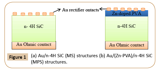
Figure 1: (a) Au/n-4H SiC (MS) structures (b) Au/(Zn-PVA)/n-4H SiC (MPS) structures.
In order to obtain the I-V, C-V and G/-V measurements for both MS and MPS structures, they were mounted on a copper (Cu) holder with the help of silver paste and electrical measurements were made to the upper electrodes by the use of tiny silver coated Cu-wires with silver paste. The measurement system was also given in Figure 2. The thickness of (Zn-PVA) (di) was determined as 50 nm from the high frequency (1MHz) C-V plot of the interlayer capacitance (Ci=εro A/di) at the strong accumulation region. As shown in Figure 2, the C-V and G/ω-V measurements were performed by the use of a computerized HP 4192A LF impedance analyzer (5 Hz-13 MHz) at low (1 kHz) and high (1 MHz) frequencies. On the other hand, the I-V measurements were performed by the use of a Keithley 2400 I-V source-meter. In addition, all measurements were carried out in dark with the help of a microcomputer through an IEEE-488 AC/DC converter card in the JANES-475 Cryostat at about 10-3 Torr to avoid an external noise or other environmental effects (Figure 2).
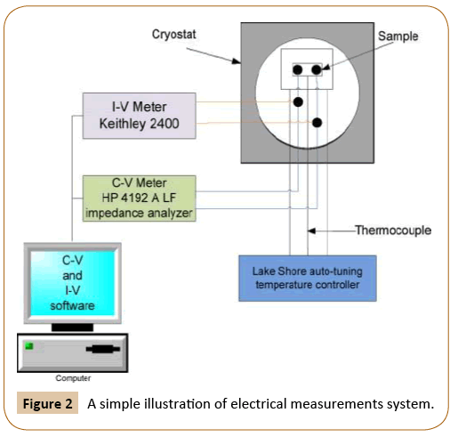
Figure 2: A simple illustration of electrical measurements system.
Results and Discussion
The forward and reverse bias current-voltage (I-V) characteristics
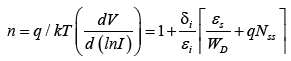
In order to determine whether or not a MS structure with modified PVA interfacial layer doped by Zn nanoparticles and without an interfacial layer has the ideal diode behavior, its experimental results at forward bias I-V characteristics and low or intermediate voltage (V3kT/q) can be analyzed according to thermionic emission (TE) theory [18-20].
 (1)
(1)
The pre-factor or the first part of the eqn. (1) represent the saturation current (Io) calculated from straight line intercept of LnI at V=0, A* is the effective Richardson constant (146 A.cm-2K-2 for n-type 4H SiC, A is the rectifier/Schottky contact area, T is the absolute temperature in K, VD is the voltage drop across the junction ad n is the ideality factor [19], and the other quantities are well known in the literature. Figure 3 shows the experimental reverse and forward bias I-V characteristics for MS and MPS type structures at room temperature. As shown in Figure 3, both MS and MPS type structures have a rectifying behavior with exponential increase of the current showing in the forward bias and weak voltage dependence in the reverse bias regions. The value of I0 was evaluated from the intercept of the linear region of LnI-V plots, whereas the value of n was evaluated from its slope for both structures according to the following equation [18,19].
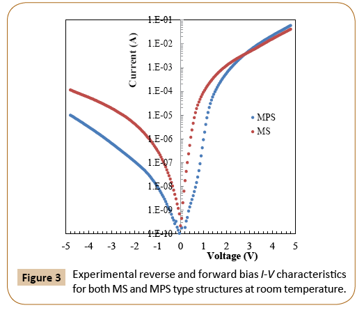
Figure 3: Experimental reverse and forward bias I-V characteristics for both MS and MPS type structures at room temperature.
 (2)
(2)
Where, δi represent the thickness of interlayer, WD represent the depletion layer width, Nss represent the surface states/traps, εi and εs represents the permittivity of modified PVA interfacial layer doped by Zn nanoparticles and semiconductor, respectively.
Now, the value of ΦBo was calculated by using theoretical value of A* and extrapolated Io values as following equation for two type structures [20].
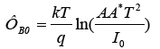 (3)
(3)
Figure 3, LnI vs. V plot of the MPS structure shows two linear regions with different slopes whereas for MS structure this plot has one linear region in the intermediate biases. For the MPS structure, these regions are belonging to low bias voltages (3kT/q ≤ V ≤ 0.55V) and intermediate bias voltage regions (0.55V ≤ V ≤ 1.30 V), respectively. Such two linear regions for MPS structure are known two parallel diodes model with different BH [31]. In addition, in the enough high forward-bias voltages, Figure 3 plot shows for both MS and MPS structure deviation from linearity due to the existence of Rs. Table 1, shows the values of I0, n and ΦB0 for MS and MPS structures were found from the first region as 1.90 × 10⁻¹¹A, 3.854, 0.906 eV and 7.08 × 10⁻¹⁰A, 3.24, 0.80 eV, respectively. These high values of n for two structures at room temperature can especially be due to the existence of native or deposited interlayer, the spatially distribution of Nss, and the exist of many distribution of low BHs or patches an average BH [8,14,18-20]. These results refer to the values of n and leakage current at (-6 V) for the MPS with (Zn doped-PVA) interfacial layer are lower than those of the MS attributed to the passivity role of Zn-PVA interfacial polymer layer. Similarly, the rectifying rate (R=IF/IR) at ±6V for the MPS structure is 15.5 times higher than MS structure (Figure 3 and Table 1).
Table 1 The experimental results values for some electrical parameters obtaind from the forward bias I-V characteristics for MS and MPS structure at room temperature.
| Samp. |
I0(A) |
n(I-V) |
ΦB0(I-V) (eV) |
Rs(dV/dln(I)-I) (Ω) |
Rs(H(I)-I) (Ω) |
RR(±6V)(=IF/IR) |
Rs(I-V) (Ω) |
Rsh(I-V)(Ω) |
| MS |
2.91 × 10⁻¹¹ |
3.854 |
0.806 |
27.03 |
89.305 |
347 |
49.4 |
2.4 × 10⁷ |
| MPS |
7.08 × 10⁻¹⁰ |
3.241 |
0.815 |
171.72 |
196.79 |
5390 |
22.1 |
9.5 × 10⁸ |
As can be seen in eqn. (2), for MPS type structure or diode has Nss in equilibrium state with semiconductor (di ≥ 3 nm) and interfacial layer, the experimental results value of n becomes greater than 1 and dependent on applied bias voltage. Thus, Nss can be calculated from the forward bias I-V characteristics by taking into account voltage dependent effective BH (Φe) and ideality factor n(Vi) by using following relations [20,27,32]:
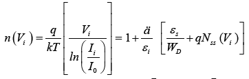 (4a)
(4a)
 (4b)
(4b)
where β is the voltage coefficient of the effective BH used in the ΦB0 ( β=dΦe/dV=1-1/n(V)). In calculations, the value of δ is taken as 20Å for native SiO2 and 500 Å for (Zn-doped PVA) layer respectively. WD is the width of the space charge region (≈3.87 × 10⁻⁵ cm which can be calculated from the linear part of reverse bias C-2 vs. V plot at 1 MHz). The value of εs was taken as13.1εo for 4H SiC, the values of εi was taken as 3.8εo for SiO2 and 8.47εo for Zn-doped PVA. The voltage dependent n(Vi) for both structures at room temperature are obtained by using eqn. (4) and shown in Figure 4. the experimental results value of n at intermediate bias voltage (for the linear region of LnI vs. V plots) is almost constant, but it becomes increase with increasing voltage almost linearly at enough high forward bias voltages for two diodes.
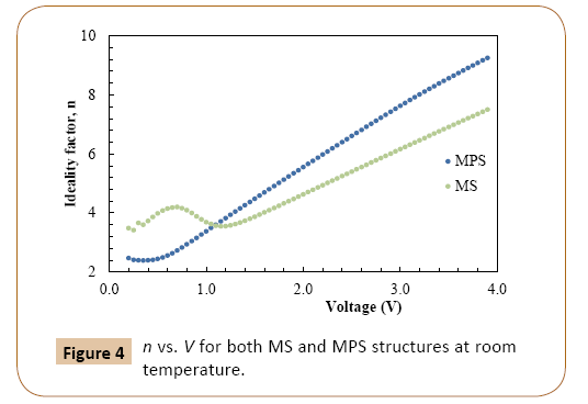
Figure 4: n vs. V for both MS and MPS structures at room temperature.
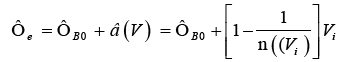
In addition, the expression for the Nss that is entirely governed by the semiconductor suggested by Card and Rhoderick can be simplified as follows [32].
 (5a)
(5a)
The energy level of Nss with respect to the bottom of the conduction band for n-type semiconductor is given by [7,21]
 (5b)
(5b)
From eqn. (4), it's clear that the value of Φe increases by increasing applied forward bias voltage because of the increase in quasi- Fermi energy level of majority carriers on the semiconductor side. Thus, the value of Nss was calculated by using eqn. 5(a) and 5(b) and was given in Figure 5 for both structures. As can be seen clear in Figure 5, the values of Nss increase from the mid-gap of 4H SiC towards the bottom of conduction band (Ec). Thus the values of Nss for the MPS are much lower like n and leakage current compared to the MS because of the saturation of dangling bonds or the passivity role of (Zn doped-PVA) interfacial layer. These results shows a grown of a modified PVA interfacial layer doped by Zn nanoparticles between metal and semiconductor instead of conventional SiO2 can increases the quality and performance of the MS and MIS type structures (Figure 5).
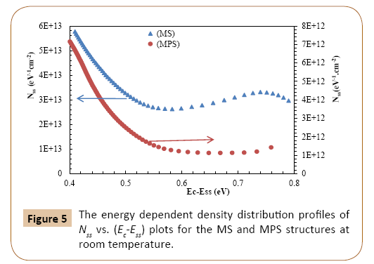
Figure 5: The energy dependent density distribution profiles of Nss vs. (Ec-Ess) plots for the MS and MPS structures at room temperature.
Usually, the forward bias I-V plot for MS, MIS and MPS structures is linear on semi-logarithmic scale at intermediate forward bias voltage (V≥3kT/q), but there it becomes deviation from linear state especially because of the exist of Rs and polymeric interfacial layer. Furthermore, the experimental values of Nss and resistance of the interlayer will be added to the resistance of epitaxial and so leads to deviate from linearity at enough high forward biases [17]. There are several methods to determine the value of Rs in the literature [18-20,22-24]. In this study, Rs has been calculated by applying the Cheung’s method [24]. by using this method, the forward bias I-V relation with Rs value can expressed as:
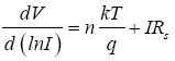 (6)
(6)
and
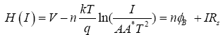 (7)
(7)
Both the dV/d(lnI) vs. I and H(I) vs. I plots were drawn by using eqns. (6) and (7) for the MS and MPS structures ant they were given in Figures 6 and 7, respectively. As shown in Figures 6 and 7, these two plots have a good linear range for two structures. Thus, a plot of dv/dln I vs. I will give the values of Rs as the slope and n values which determined from eqn. (6) which represent the y-axis intercept (=nkT/q), of these plots respectively. Similarly, the slope of H(I) vs. I plot (Figure 7) will provide a second way for determination of Rs, which produce a check the uniformity of this approach. From eqn. (7), the values of Rs and ΦB were calculated and obtained from the slope and the intercept of y-axis (=nΦB) of these plots for two structures, respectively. The values of n which are calculated from Cheung function acorrding to eqn. (6) are considerably higher than those extractes from eqn. (2). Figure 4, shows an expected situation due to the increase of n with applied bias voltage. The voltage dependence of structure resistance (Ri) is also obtained by applying Ohm’s law (Ri=dVi/dIi) and represented inset in Figure 3 for MS and MPS type structure. As shown in this figure, the real values of Rs and Rsh for both two structures agree to enough high forward bias voltage (6V) and enough low or zero bias voltages, respectively. As seen in Table 1, the experimental result of Rsh value for MPS structure is 39.99 times higher as compare with Rsh value for MS structure. The experimental values of Rs that obtained from Cheung’s functions and Ohm’s law for two structures were represented in Table 1. The discrepancy between Rs from these methods is the result of voltage dependence of it like ideality factor and BH.
Figure 6: (a) dV/dln(I) vs. I for MS structure. (b) dV/dln(I) vs. I for MPS structure.
Figure 7: (a) H(I) vs. I for MS structure. (b) H(I) vs. I for MPS structure.
The forward and reverse bias C-V and G/ω-V characteristics
The capacitance and conductance measurements (C-V and G/ω-V) respectively were applied at both low (1 kHz) and high (1 MHz) frequencies by using HP 4192A LF Impedance Analyzer. According to Nicollian and Brews [22], at enough low frequencies, almost of all surface states can follow the external alternating ac signal easily and so yield an excess Cex. and Gex./ω to the real values of them, but at high frequencies these states/traps impossible follow the ac signal. For this purpose, the C-V and G/ω-V plots of the MS and MPS structures were drawn at low frequency 1 kHz and high frequency 1 MHz. shows the C-V characteristics for MS and MPS Figure 8a and 8bstructures at 1 kHz and 1 MHz, respectively, and these plots have three regions (inversion, depletion and accumulation) both low and high frequency. C-V characteristic has shown clearly that the anomalous peak at the accumulation region due to the effect of Rs and native SiO2 and (Zn-doped PVA) interfacial layer rather than Nss. It is clear that the magnitude of anomalous peak inversely related to frequency due to the effect of Nss. This kind of peak behavior can be attributed to the particular density distribution of Nss and remodeling and restructure of them under applying electric field [32-34]. As seen in Figure 8a and 8b the value of capacitance of both structures are extremely sensitive to the Nss, interfacial layer and Rs, but Nss shows an effective behavior especially at inversion and depletion regions, whereas Rs shows an effective behavior only at accumulation region.
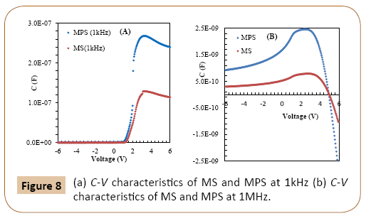
Figure 8: (a) C-V characteristics of MS and MPS at 1kHz (b) C-V characteristics of MS and MPS at 1MHz.
As seen in Figure 8b, at 1 MHz, C value increases with increasing voltage until accumulation region after that it suddenly decrease until goes to negative due to the effect of Rs, but at 1 kHz, this negative capacitance (NC) behavior becomes disappear. Because, the effect of Rs on C-V and G/ω-V plots can be neglected low at low frequencies, but it becomes very effective at high frequencies contrary to Nss. The general consensus on NC in the accumulation region is due to the existence of Nss and their relaxation time (τ), Rs, the contact injection and minority carrier injection [35,36]. In addition, according to Butcher et al. [37] and Huang et al. [38], NC behavior can be attributed to technical problems of devices, such as parasitic inductance or accuracy of calibration, respectively (Figure 8).
In general, the NC has been referred to as “abnormal” or “anomalous” behavior in the literature [33]. The C value is a differential effect of charge Q with respect to junction voltage Vj, i.e. C=dQ/dVj Zhu et al. [39]. Furthermore, by increasing forward bias voltage the C values reach to a maximum value and after certain voltage it started rapidly in decreasing until reach to negative value [35,39,40]. C-V and G/ω-V plots for MS and MPS structures at 1 MHz were drawn to see the inductive behavior in these structures in Figure 9a and 9b, respectively, which explain how the G/ω value increases for two structures with increasing frequency both at depletion and accumulation region, but at accumulation region contrary to G/ω, the value of C reaches a peak value and then goes to negative value at strong accumulation region. In addition, the minimum value of C represent the maximum value of G/ω. NC exhibits a decrease in electronic charges on electrodes with an increasing bias voltage and such behavior of C and G/ω is known as “inductive behavior” in the literature [33-40] (Figure 9).
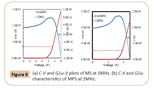
Figure 9: (a) C-V and G/ω-V plots of MS at 1MHz. (b) C-V and G/ω characteristics of MPS at 1MHz.
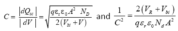
The variation in C at the reverse bias or inversion region, the C-2-V plot of the MS and MPS structures for 1 MHz are given in Figure 10. As shown in Figure 10, the C-2-V plot for two different type structures has a perfect linear region in the wide range of reverse bias voltage. At elevated frequencies (f ≥ 1MHz), the depletion layer capacitance of MS and MPS type structures can be expressed as following [18-20].
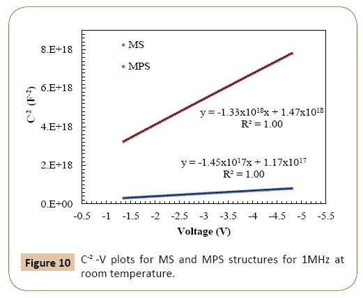
Figure 10: C-2 -V plots for MS and MPS structures for 1MHz at room temperature.
 (8)
(8)
In eqn. (8), A represent the rectification contact area, VR represent the reverse-bias voltage, Vbi represent the built-in voltage at zero bias, Nd represent the donor concentration atoms in 4H SiC, εr represent the permittivity of semiconductor and εo represent the permittivity of free space or vacuum. The values of Vo, Nd, EF, Φb (C-V) and depletion layer width (WD) are calculated from the intercepts and slopes of the C-2-V plot for each structure using following relations [18-21]:
 (9)
(9)
 (10)
(10)
The value of EF can be calculated from the conduction band edge for n-type semiconductor in the neutral region of n-4H SiC by using following relation as [18,19]:
 (11)
(11)
Where, Nc is the effective density of states in n-4H SiC conduction band. The experimental values Vo, Nd, EF, ΦB and WD were obtained and arranged as in Table 2.
Table 2 The expermental values of some parameters at the linear parts of the reverse bias C-2 vs. V plots for MS and MPS structure at room temperature.
| Sample |
V0
(V) |
Nd(cm-3) |
EF(eV) |
ΦB(eV) |
WD(cm) |
| MS |
0.807 |
8.373 × 10¹⁶ |
0.123 |
0.955 |
1.249 × 10⁻⁵ |
| MPS |
1.105 |
9.128 × 10¹⁵ |
0.179 |
1.309 |
3.781 × 10⁻⁵ |
As can be seen in Tables 1 and 2, the ΦB0(C-V) value which calculated from the reverse bias C-V characteristics is higher than ΦB0 (I-V) which calculated from the forward bias I-V characteristics due to the nature of measurement methods. In other words, the values of BH obtained from two techniques are not always the same in bias voltage. It is well known that the apparent BH from metal side to semiconductor side is higher than at about EF from semiconductor to metal sides. This discrepancy between ΦB0 (C-V) and ΦB0 (I-V) is also the result of the in-homogeneities of BH and polymeric interfacial layer at M/S interface.
The profile of Rs as voltage dependent was also calculated by using eqn. (12) for the C-V and G/ω measurements by applying Nicollian and Brews method at 1MHz to explain how Rs effects on both C-V and G/ω-V characteristics for MS and MPS structure and were given in Figure 11 [22].
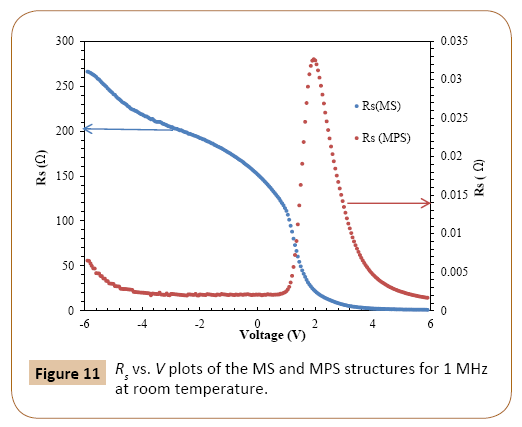
Figure 11: Rs vs. V plots of the MS and MPS structures for 1 MHz at room temperature.
 (12)
(12)
As shown in Figure 11, the value of Rs at accumulation region is almost independent from applied bias voltage and so it is representing to the real value of Rs for two type structures. Thus, the real value of Rs for MS and MPS structure was found as 1.09 Ω and 1.63 Ω at 6 V, respectively. The value of Rs for MPS structure is also lower than the MS structure and these values of Rs are more suitable for an electronic device. The peak behavior in Rs vs. V plot for MPS structure can be caused by particular distribution of Nss at (Zn doped-PVA)/n-4H SiC interface. Because, at peak position, the charge carriers may be trapped due to higher value of Nss and at certain high forward biases voltage the value of Rs will decrease due to decreasing of charge carriers at traps or states. Finally, in order to see the charges at surface states or traps on the C-V and G/ω-V plots, the profiles of Nss vs. V was also calculated from the high-low frequency (1MHz-1 kHz) capacitance (CHF-CLF) technique using following relation for both structures and they were given in Figure 12.
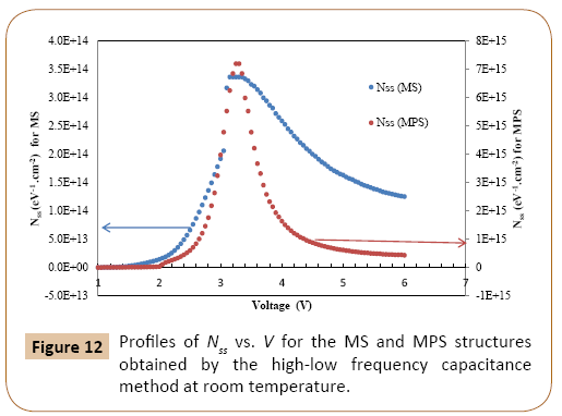
Figure 12: Profiles of Nss vs. V for the MS and MPS structures obtained by the high-low frequency capacitance method at room temperature.
 (13)
(13)
In eqn. (13), Ci is the interfacial layer capacitance and was obtained by using the Cma and Gma/ω values at strong accumulation region at 1 MH by using following relation [22].
 (14)
(14)
As seen in Figure 12, the density of Nss for MS and MPS type structures shows a peak value due to a special density distribution of Nss and their remodeling and restructure under electric field. As a result, the values of Nss obtained high-lowfrequency capacitance method for MPS structure are also lower than MS structure at accumulation region, but the distribution of Nss varied from region to region due to their special distribution between interfacial layer and semiconductor. Furthermore, Figure 12 show a peak value of Nss at about 3V for both MS and MPS structures with higher value for MPS 10 times than MS structure and then at higher voltage V ≥ 3 the value of Nss exponentially decreases from conduction band to mid-gap with increasing applied biasing voltage in different ratio for both structures. These results indicated the electrical parameters of these structures to be quite dependent on voltage as well as interfacial polymeric layer. When the main electrical parameters of MS and MPS structure are compared; the values of ideality factor, leakage current, Rs, ΦBo and Nss for MPS structure are considerably lower than the MS structure. However, the values of Rsh and RR for MPS structure are considerably higher than the MS structure due to the passivity role of Zn-PVA interfacial polymer layer. As a result, we can say that the (Zn doped-PVA) polymer material can be applied as an interfacial layer instead classical SiO2 insulation layer to get better quality or performance of MS structure.
Conclusion
In this study, how the effect of modified PVA interfacial layer doped by Zn nanoparticles on the electrical parameters was evaluated and investigate after fabrication of both Au/n-4H SiC (MS) and Au/(Zn-doped PVA)/n-4H SiC (MPS) structures with the same substrate -4H SiC wafer. The main important electrical parameters are obtained from forward and reverse I-V, C-V and G/ω-V characteristics at room temperature to compare of them. These results show that the main electrical parameters of these MS and MPS structures are considerably dependent on voltage as well as interfacial layer.
The comparison between the two structures showing the that the higher values of BH obtained from the reverse bias C-V data as compare with the forward bias I-V data for the two structures due to the nature of the used of measurement technique. The high values of n for two structures were caused by the existence of the native and doped interfacial layer, lower barriers or patches at around mean value of BH and the existence of Nss at interfacial layer/n-4H SiC interface. The profiles of Nss vs. V was measured by using the forward bias I-V data by taking into account the voltage dependent BH and n for these two structures. The values of Nss increase an exponential from the mid-gap of n-4H SiC toward the bottom of its Ec. On the other hand, the profile of Rs for these structures was measured from the C-V and G/ω-V data by applying Nicollian and Brews method. These obtained experimental results are confirmed that the effect of presence of Nss, Rs, and the interfacial layer is most influential on the electrical parameters of the MS and MPS structures. In conclusion, when the main electrical parameters of both structures are compared; the values of n, leakage current, Rs, ΦBo and Nss for MPS structure are lower than the MS structure, but the values of Rsh and RR for MPS structure are higher than the MS structure due to the passivity role of Zn-PVA interfacial polymer layer. As a result, we can say that the (Zn doped-PVA) polymer material when applied as interfacial layer instead of classical SiO2 insulator layer, this will improve the quality or performance of MS structure.
Acknowledgments
This study is corroborative by Süleyman Demirel University (project no: 4614-D2-16).
References
- Reddy MSP, Kang HS, Lie JH, Reddy VR, Ja Jang S (2014 Electrical Properties and the Role of inhomogeneities at the Polyvinyl Alcohol/n-InPSchottky Barrier Interface.ApplPolymSci 131:139773-10.
- GülüÖ, AydoğanŞ, TürütA (2012) Electronic parameters of high barrier Au/Rhodamine-101/n-InpSchottky diode with organic interlayer. Thin Solid Films 520: 1944-1948.
- AltındalYeriskin S,BalbaşıAM (2016)Tataroğlu, Frequency and voltage dependence of dielectric properties, complex electric modulus, and electrical conductivity in Au/7% graphene doped-PVA/n-Si (MPS) structures. J ApplPolymSci 133: 43827.
- Reddy VR (2014) Electrical properties of Au/polyvinylidenefluoride/n-InPSchottkydiode with polymer interlayer. Thin Solid Films 556: 300.
- TaşçıoğluÄ°, TüzünÖzmenÖ, Sağban HM, YağlıoğluE, AltındalŞ (2017) Frequency Dependent Electrical and Dielectric Properties of Au/P3HT: PCBM: F4-TCNQ/n-Si Schottky Barrier Diode. J Electron Mater 46: 2379-2386.
- Özdemir AF, Aydın SG, Aldemir DA, Görsoy SS (2011) Electrical and optical properties of p-type silicon based on polypyrrole-derivative polymer. Synth Met 161: 692-697.
- Altındal S, Sarı B, Ünal HI, Yavas N (2009) Electrical Characteristics of Al/PolyindoleSchottky Barrier Diodes. I. Temperature Dependence. J Appl PolymSci 113: 2955-2961.
- BilkanÇ, Zeyrek S, San SE, AltındalŞ (2015) A compare of electrical characteristics in Al/p-Si (MS) and Al/C20H12/p-Si (MPS) type diodes using current-voltage (I-V) and capacitance-voltage (C-V) measurements.Mater Sci and Semicon Process 32: 137-144.
- Moraki K, Bengi S, Zeyrek S, Bülbül MM, AltındalŞ(2016) Temperature dependence of characteristic parameters of the Au/C20H12/n-Si Schottky barrier diodes (SBDs) in the wide temperature range. J Mater Sci: Mater Electron 28: 3987-3996.
- ҪicekӦ,UsluTecimer H,Tan SO, Tecimer H, AltındalŞ, et al. (2016) Evaluation of electrical and photovoltaic behaviours as comparative of Au/n-GaAs (MS) diodes with and without pure and graphene (Gr)-doped polyvinyl alcohol (PVA) interfacial layer under dark and illuminated conditions. Composites Part B 98: 260.
- DemirA,Yücedağİ, Ersöz G, AltındalŞ, BarazN, Kandaz M (2016) A ComparativeStudy on the Main Electrical Parameters of Au/n-Si,Au/Biphenyl-CuPc/n-Si/and Au/Biphenylsubs-CoPc/n-Si/Type SchottkyBarrier Diodes.J. Nanoelectron and Optoelectron 11: 620-625.
- Bülbül MM, Bengi S, DökmeÄ°, AltındalŞ,Tunç T (2010)Temperature dependent capacitanceand conductance-voltage characteristics of Au/polyvinyl alcohol(Co,Zn)/n-Si Schottky diodes, J. Appl. Phys., 108: 34517-1-034517-6.
- AltındalŞ, UsluH (2011)The origin of anomalous peak and negative capacitance in the forward bias capacitance-voltage characteristics of Au/PVA/n-Si structures.J Appl Phys 109: 074503-1-074503-7.
- Tunc T, AltındalŞ, UsluI, DökmeI (2011) Temperature dependent current–voltage (I–V) characteristics of Au/n-Si (111) Schottky barrier diodes with PVA(Ni,Zn-doped) interfacial layer. Mat SciSemProc 14: 139-145.
- Gökçen M, Tunç T,AltındalŞ,UsluÄ° (2012) Electrical and photocurrent characteristics of Au/PVA (Co-doped)/n-Si photoconductive diodes. Mater Sci and Eng B 177: 416-420.
- Casady JB, Johnson RW (1996) Status of silicon carbide (SiC) as a wide-bandgap semiconductor for high-temperature applications: A review, Solid State Electron 39: 1409.
- Sochacki M, Kolendo A, Szmidt J, Werbowy A (2005) Properties of Pt/4H-SiC Schottky diodes with interfacial layer at elevated temperatures. Solid State Electron 49: 585.
- SzeSM (1981) Physics of Semiconductor Devices, John Wiley and Sons, Toronto.
- Rhoderick EH (1978) Metal-Semiconductor Contacts, Oxford University Press.
- Sharma BL (1984) Metal-semiconductor Schottky Barrier Junctions and their applications, Plenum Press, NewYork and London.
- CardHC, Rhoderick EH (1971) Studies of tunnel MOS diodes I. Interface effects in silicon Schottky diodes. J Phys D-Appl Phys 4: 1589-1601.
- Nicollian EH, Brews JR (1982) MOS Physics and Technology, Wiley, New York.
- Norde H (1979)A modified forward Iâ€ÂÂÂÂV plot for Schottky diodes with high series resistance. J ApplPhys, 50: 5052-5053.
- Cheung SK, Cheung NV (1986) Extraction of Schottky diode parameters from forward currentâ€ÂÂÂÂvoltage characteristics Appl Phys Lett 49: 85-87.
- Tung RT (2001) Recent advances in Schottky barrier concepts. MatSciEngineerring 35: 1.
- Werner JH, Guttler H (1991) Barrier inhomogeneities at Schottky contacts. J ApplPhys, 69: 1522-1533.
- Alialy S, AltındalŞ, Tanrıkulu EE, Yıldız DE (2014) Analysis of temperature dependent current-conduction mechanisms in Au/TiO2/n-4H-SiC (metal/insulator/semiconductor) type Schottky barrier diodes.J ApplPhys, 116: 083709.
- Kimoto T, Cooper JA (2014)Fundamentals of Silicon Carbide Technology(1.st Edn) 2014 John Wiley & Sons Singapore.
- Kamoun O, Boukhachem A, Yumak A, Petkova P, Boubaker K, et al. (2016) Europium incorporation dynamics and some physical investigations within ZnO sprayed thin films, Materials Science in Semiconductor Processing 43: 8-16.
- Singh PK, Gaur MS, Chauhan RS (2015) Dielectric properties of sol–gel synthesized polysulfone–ZnO nanocomposites.JTherm Anal Calorim 122: 725.
- Demirezen, Kaya A, VuralÖ, AltındalŞ (1971) The effect of Mo-doped PVC+ TCNQ interfacial layer on the electrical properties of Au/PVC+ TCNQ/p-Si structures at room temperature, ,Materials Sci. in Semicond. Proces., 33 (2015)140–148.32. H.C. Card, E.H. Rhoderick, Studies of tunnel MOS diodes I. Interface effects in silicon Schottky diodes.J Phys D: ApplPhys 4: 1589.
- Demirezen S, Kaya A, Yerişkin SA, Balbaşı M, Usluİ (2016) Frequency and voltage dependent profile of dielectric properties, electric modulus and ac electrical conductivity in the PrBaCoOnanofiber capacitors. Results in Phys 6: 180.
- Arslan E, Bütün S, Şafak Y, Uslu H, TaşçıoğluÄ°, et al. (2011) Electrical characterization of MS and MIS structures on AlGaN/AlN/GaNheterostructures, Microelectron. Rel 51: 370.
- Uslu H, Altındal Ş, Tunç T,Uslu Ä°, Mammadov TS (2011) The illumination intensity and applied bias voltage on dielectric properties of au/polyvinyl alcohol (Co, Znâ€ÂÂÂÂdoped)/nâ€ÂÂÂÂSi Schottky barrier diodes, J. of Appl Polym Sci 120: 322.
- Ershov N, Buchanan M, Wasilewski ZR, Jonscher AK (1998) Negativecapacitance effect in semiconductor devices. IEEE Transactions on Electrical Devices 45: 2196.
- Werner J, Levi AFJ, Tung RT, Anzlowar M, Pinto M (1988) Origin of the excess capacitance at intimate Schottky contacts Phys Rev Lett 60: 53-56.
- Butcher KSA, Tansley TL, Alexiev D (1996)An instrumental solution to the phenomenon of negative capacitances in semiconductors. Solid-State Electron 39: 333-336.
- Huang XL, Shin YG, Lim KY, Suh EH, Lee HJ, et al. (1997) Thermally induced capacitance and electric field domains in GaAs/Al0.3Ga0.7As quantum well infrared photo detector. Solid-State Electron 41: 845-850.
- Zhu CY,Feng LF, Wang CD, Cong HX, Zhang GY,et al. (2009) Negative capacitance in light-emitting devices.Solid-State Electron 53: 324–328.
- BilkanÇ, Gümüş A, Altındal Ş (2015) The source of negative capacitance and anomalous peak in the forward bias capacitance-voltage in Cr/p-siSchottky barrier diodes. (SBDs) Mater Sci Semi condProces 39: 484-4911.