Vega O1,2*, Wong F3, Vega E4, Luciano J4, Rodriguez S4, Pinto NJ4 and Rosa LG2,4
1University of Puerto Rico-Rio Piedras, Department of Physics, Natural Sciences Faculty Department of Physics, PO BOX 70377 San Juan, PR 00936 USA
2University of Puerto Rico, Institute for Functional Nanomaterials, PO Box 233343, San Juan, PR 00931 USA
3Turabo University, Department of Environmental Chemistry, PO BOX 3030, Gurabo Puerto Rico, 00778 USA
4University of Puerto Rico-Humacao, Department of Physics and Electronics, Av. Jose Aguiar Aramburu Road 908 km 1.2, Humacao, PR 00792 USA
*Corresponding Author:
Omar Vega
Department of Physics and Electronics
University of Puerto Rico-Humacao
Ave. José E. Aguiar Aramburu Road
908 Km 1.2 PR 00791 USA
Tel: 787-413-7367
E-mail: omar.vega3@upr.edu
Received Date: June 03, 2017; Accepted Date: June 15, 2017; Published Date: June 25, 2017
Citation: Vega O, Wong F, Vega E, Luciano J, Rodriguez S, et al. (2017) Electronic Transport and Anisotropic Conductivity Behavior on PEDOT:PSS Nanoribbons and Nanostructuring Modification by Atomic Force Microscope Nanoshaving. Polym Sci. Vol. 3 No. 1: 6.
Keywords
Dip-pen; Nanolithography; Nanoshaving; Atomic Force Microscopy (AFM); Poly(3,4-ethylenedioxythiophene) polystyrene sulfonate (PEDOT-PSS)
Introduction
The field of conjugated polymer semiconductors developed from a fundamental laboratory discovery into a manufacturing technological material for a range of thin-film nanostructures for electronics applications [1-3], which benefits from the compatibility of polymers with large-area, low-cost, room temperature solution processing, structural flexibility and directwrite printing. Since their discovery [4,5], polymer semiconductor applications now include emissive light-emitting diodes, flat panel displays, and low-cost thin film transistor circuits on flexible substrates [6]. Recently, it has become clear that some general manufacturing methodologies of polymer electronics, which have been successfully applied to develop conventional, thin-film electronic devices, might also open up a new pathway for functional nanostructures and devices. Fabrication methods like electro spinning provide these advantages of fabricating nanostructures like nanofibers and nanoribbons [7-10].
Utilizing nanofabrication methods of AFM Nanolithography, Nanoshaving, on Nanoribbons of poly(3,4-ethylenedioxythiophene) polystyrene sulfonate (PEDOT-PSS) by nanoshaving, an atomic force microscopy nanolithography technique [11-13], we will explore the limits and flexibility of this material. This process involves an AFM tip under a relatively high force load to shave away or displace material. The fabrication of nanostructure methods of lithography has typically been achieved on materials by more standard methods like electron beam lithography, X-ray and UV photolithography, self-assembly and recently nano- and micro-imprint (“stamped”) lithography [14-17]. Other methods for fabrication are available, e-beam lithography, x-ray and UV photolithography. But due to the aggressive beams and high photon energy they may severely damage our material on the surface and deteriorate the performance of our organic semiconductor [18-21]. Self-assembly methods, on the other hand, enable high fabrication output, but suffer from poor or limited control over feature size. Pervious nano, micro fabrication and lithography on poly(3,4-ethylenedioxythiophene) polystyrene sulfonate have demonstrated high-density arrays of organic semiconductors, showing a large throughput and high control of the features size [22-25]. On the other hand, self-assembly methods, enable high fabrication output, but suffer from poor or limited control over feature size [22-25].
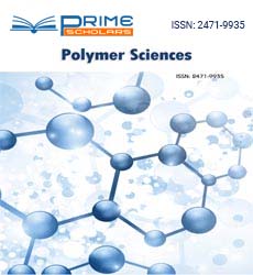
Nanoribbons of organic semiconductor salts, poly(3,4- ethylenedioxythiophene) polystyrene sulfonate (PEDOTPSS), have been deposited on silicon dioxide (SiO2) by the electrospinning technique. It is possible to “shave” or mechanically displace small regions of the polymer nanoribbon by using atomic force microscopy (AFM) nanolithography techniques such as nanoshaving, leaving swaths of the surface cut to the depth of thickness of the nanoribbon. By placing the nanoribbon between two electrode pads with a 10 μm gap, for the first time we performed nanoshaving on the nanoribbon by removing portions of the PEDOT-PSS nanoribbon: Figure 1a. An in-situ transport measurement was performed of the nanoribbons’ dependence on the remaining cross section.
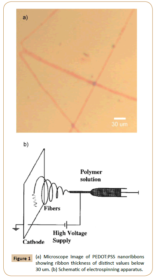
Figure 1: (a) Microscope Image of PEDOT:PSS nanoribbons showing ribbon thickness of distinct values below 30 um. (b) Schematic of electrospinning apparatus.
Nanoribbon Preparation
Utilizing basic elements of electro spinning apparatus, a hypodermic syringe (0.5 cm3 tuberculin syringe) a high voltage power supply (Gamma Research) and a syringe pump (Cole Parmer) as shown in Figure 1b. The needle of this syringe was connected to the power supply, with the cathode (Al foil) grounded at about 20cm.The PEDOT-PSS poly(3,4-ethylenedioxythiophene) polystyrene sulfonate was purchased from Bayer Corp and used as-received and the solution and a 1 wt.% of polyethylene oxide (PEO-plasticizer) was prepared and it was used to produce the nanoribbons via electrospinning [7-10,26]. This solution was placed in the syringe (about 0.5 mL) once the power supply was turned on the syringe pump was set at one drop per 10s. Once the power supply reached a 10kV value, the polymer droplet surpassed the surface tension it starts to jet towards the cathode in short bursts. In Figure 1a we can observe the nanoribbons deposited on the Si/ SiO2 substrate. In this low magnification image, we can see that some of the ribbons appear to be flattened; this may be due to the incomplete solvent evaporation prior to it striking the cathode. These nanoribbons where isolated by intercepting the jet flow of the polymer with the passing of the Si/SiO2 between the syringe and the Al cathode. Electrospinning PEDOT-PSS without PEO did not yield any ribbons.
Atomic Force Microscopy (AFM) Characterization and Nanoshaving
Nanostructuring and imaging were both carried out using a NanoInk Inc. DPN 5000 System. The process of nanoshaving has been described extensively elsewhere [11-13,27-29]. Briefly, an AFM tip is used, at low force, to image the surface morphology and to select a region for nanolithography. Mechanical scratching or nanoshaving, Figure 2, may be the most straightforward way of performing nanolithography with AFM; in this process, the tip is employed to displace materials from the sample surface, creating pits or trenches surrounded by walls consisting of the initial substrate material. It has been successfully applied to surfaces of metals, semiconductors and polymers. A necessary consideration in creating reproducible patterns is the durability of the tip itself, which is prone to deformation and contamination after repeated scanning. To avoid excessive wear, it has been proposed that tips composed of, or coated with, hard materials (e.g. diamond) or dynamic mode AFM should be used for such experiments. Nanoshaving was performed under ambient conditions in an acoustic isolation box at 50% ambient humidity. AFM imaging was performed in contact mode, in which the tip is placed in contact with the surface. During the contact mode imaging, the load force of the tip on the surface was controlled to be less than 1 nN during imaging unless otherwise specified; while for nanoshaving, loads as large as 100 nN were used. Typical scan rates for nanoshaving were 2 and 0.5 Hz, respectively. Finally, the cross-sectional height and amplitude analyses were carried out on the acquired topographical data. The software used for the data processing was Scanning Probe Image Processor (SPIP 5.0.5).
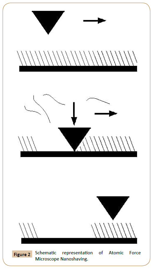
Figure 2: Schematic representation of Atomic Force Microscope Nanoshaving.
Transport Measurements
Transport characterization of the PEDOT-PSS nanoribbon (I-V) properties was measured with a Keithley 6517A electrometer in an environmental chamber with 50% humidity in air [7-10,30]. The ohmic contact to the nanoribbon was accomplished by thermally evaporating an Au pad by shadow mask of 100 μm x 100 μm area and 100 nm thicknesses on the nanoribbons (Figure 3). The square gold pads are separated by 10 μm for the electronic transport channel. The (I-V) stage was carefully mounted under the Atomic Force Microscope for in-situ measurements while measuring their (I-V).
Figure 3: (a) Schematic of nanoribbon (blue) on a SiO2 surface between two gold (Au) electrodes at 10 um separation distance. AFM imaging of lateral deflection on (b) and topography or height structural image (c) of a nanoribbon with 28 nm height and 3.7 um width.
Results and Discussion
AFM characterization: Nanoribbon thickness and aspect ratio
Nanoribbons of PEDOT-PSS poly(3,4-ethylenedioxythiophene) polystyrene sulfonate were fabricated by electrospinning methods on silicon dioxide (SiO2) substrate. Due to the random nature of the electrospinning process and the lack of precise nanoribbon dimension's control, a large number of nanoribbons and nanofibers deposited as above were sought individually by means of Atomic Force Microscope contact and non-contact methods. AFM images were undertaken at a normal applied force by the AFM probe controlled to remain below 1 nN, at ambient conditions. On clean substrates of SiO2, the surface is atomically flat with only a few atomic steps.
Measuring the height “thickness” and the width of the nanoribbon (Figure 4), if carried out to sufficient precision, is useful for determining the configuration of the molecules. The height “thickness” in particular has been a useful tool to determine molecular or structural information [11-13,27-28]. The crosssectional analysis indicates the thickness of the nanoribbon and its width, as shown in Figure 4b. As a comparison tool, we measure the width vs. height plot or aspect ratio equivalent of the nanoribbon shown in Figure 5. As shown in Figure 5, the width vs. height plot exhibits a decrease in width when the height increases between 0-7.9 nm. Around 7.9 nm height, the plot undergoes a change in the relationship, in which the width and height both increase proportionally, showing evident width minima at 1.1 um. As shown in Figure 5 inset, two-line fitting was used to calculate the intercept at 7.92 nm height at a minimal width of 1.1 um, which defines the transition from a negative slope relationship to a positive slope. From this experimental relationship, it is possible from the electro spinning fabrication method to obtain two fibers with the same width, but with two distinct heights (“thicknesses”) of the nanoribbons.
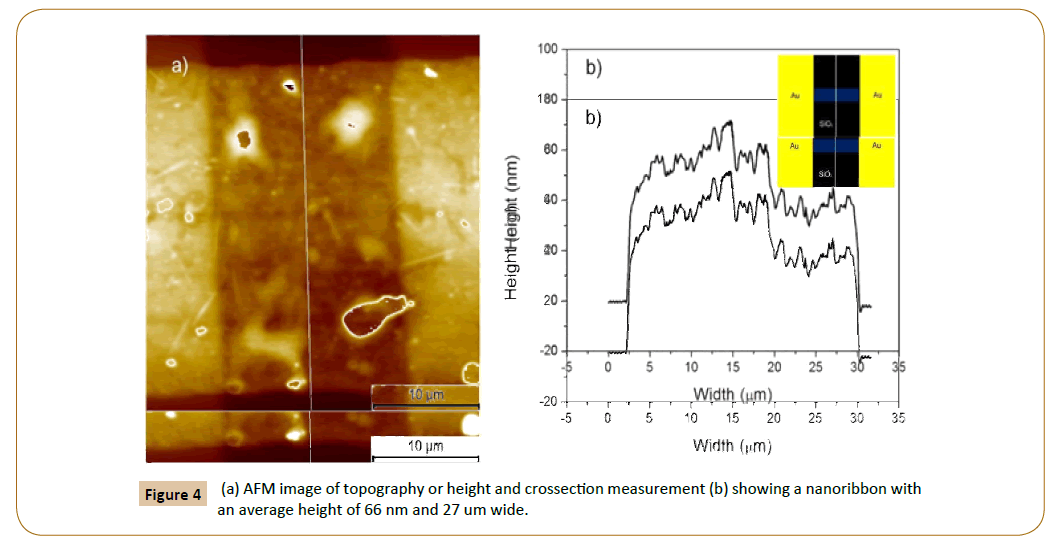
Figure 4: (a) AFM image of topography or height and crossection measurement (b) showing a nanoribbon with an average height of 66 nm and 27 um wide.
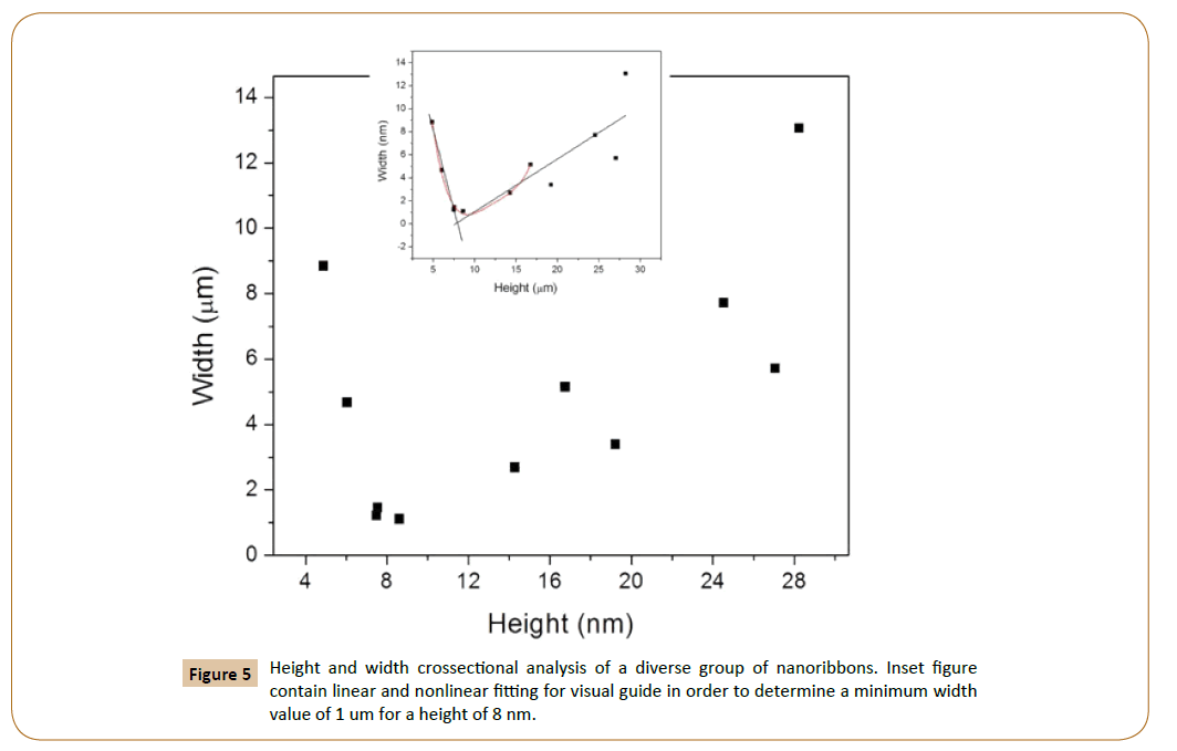
Figure 5: Height and width crossectional analysis of a diverse group of nanoribbons. Inset figure contain linear and nonlinear fitting for visual guide in order to determine a minimum width value of 1 um for a height of 8 nm.
The polymer interlayer spacing reported from crystallographic data [31-34], Figure 6, shows that the unit cell for PEDOT is ~1.4 nm along the a-axis (100) direction. The b-axis or (010) direction shows a face-to-face repetitive unit of 0.68 nm, the direction in which the plane of the thiophene ring faces each other in parallel. The c-axis 0.78 nm (001) is along the polymer chain’s main molecular axis. The polymer interlayer spacing from the nanoribbons can be estimated using Atomic Force Microscopy by defining one monolayer (1 ML) as the minimum height measured on Figure 5 to be 4.88 nm, obtained from electrospinning fabrication. This minimum value in height shown in Figure 5 to be 4.88nm is in agreement with the literature value of crystal grain size reported values between 3 nm to 5 nm [33,35,36]. A monolayer (ML) is defined by an integer number of molecular monolayers. The interlaying spacing results are shown in Table 1, with a range of values between 1.37-1.63 nm. The following range of interlaying spacing agrees with the 1.4 nm interlaying spacing along the (100) or a-axis [31,32] reported from crystallographic data. The range values obtained from the results of electrospinning (Table 1), 1.37–1.63 nm (average 1.46 nm) are also in agreement with the counter-ion chemistry and d (100) spacing correlation established by Martin [31] As shown in Table 2, the d(100) spacing reported by Martin [31], the counter-ion PSS- shows a d(100) distance of 1.46 nm.
| Nanoribbon Height (nm) |
Molecular Monolayer Integer |
d(100) nm |
| 4.88 |
3 |
1.62 |
| 6.05 |
4 |
1.51 |
| 7.53 |
5 |
1.51 |
| 8.62 |
6 |
1.44 |
| 14.3 |
10 |
1.43 |
| 16.8 |
12 |
1.4 |
| 19.2 |
14 |
1.37 |
| 24.5 |
17 |
1.44 |
| 27.1 |
19 |
1.43 |
| 28.2 |
20 |
1.41 |
| Average value d(100) |
1.46 |
Table 1: Atomic force microscopy measurements of Nanoribbon height and fitted integer of molecular monolayers with resulting polymer interlaying spacing d(100).
| Counter-ion |
d(100) nm |
| PAA- |
1.52 |
| PSS- |
1.46 |
| PTS |
1.39 |
| Cl-(NaCl) |
1.39 |
| C14SO3 |
1.37 |
| Cl-(CaCl2) |
1.33 |
| EBS |
1.32 |
| CSA |
1.29 |
| F- |
1.15 |
Table 2: d(100) Spacing of PEDOT as a function of counter-ion chemistry as reported by Martin[31]. Abbreviations: PAA-: Poly(acrylic acid), PSS-: Polystyrene Sulfonate, PTS: p-Toluene Sulfonate, EBS: 4-Ethylbenzenesulfonate, CSA: Camphorsulfonic Acid.
Electronic transport properties and crosssectional dependence
Transport measurements were performed on the nanoribbons. The nanoribbons, as described in the experimental section, were connected by thermal evaporating gold pads separated by a 10 μm gap; see Figure 4. The chosen nanoribbon of Figure 4 has an average height of 66 nm and average width of 27 um. To study the nanoribbon’s cross-sectional dependence on the electronic transport, we used nanoshaving by Atomic Force Microscopy. As described above, nanoshaving is an Atomic Force Microscopy Nanolithography technique, in which a large normal force is applied on the tip to penetrate the material and to remove or displace materials, leaving behind the exposed original substrate. Cuts as shown in Figure 7 were purposely made to change the cross-sectional area for the electronic transport on the fiber. Rectangular-shape cuts of 500 nm width were performed in sequence; for each cut, a current vs. voltage (I-V) or transport measurement was performed. The sequence of cuts and (I-V) was continued until a small portion of 500 nm x 500 nm was left in the nanoribbon, as shown in Figure 7d inset. From the measured (IV) curves, we obtained the (J-V) curve or the current density of each measurement. The current density (J = I/A) was obtained by dividing the current (I) and the remaining cross-sectional area (A) measured by AFM after each cut by nanoshaving and successful removal of material. As shown by our sequence of experiments in Figure 7, the (J-V) curves in Figure 8 show a dependence on the cross-sectional area, and an evident decrease in the conductance (G = 1/R) of the nanoribbon, where R is the resistance of the materials. On the other hand, the conductivity of the material was obtained by (σ = GL/A), with conductance (G), nanoribbon length (L) and nanoribbon cross-sectional area (A).
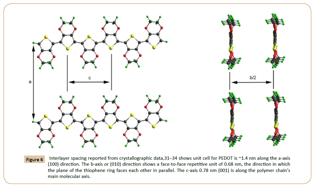
Figure 6: Interlayer spacing reported from crystallographic data,31–34 shows unit cell for PEDOT is ~1.4 nm along the a-axis (100) direction. The b-axis or (010) direction shows a face-to-face repetitive unit of 0.68 nm, the direction in which the plane of the thiophene ring faces each other in parallel. The c-axis 0.78 nm (001) is along the polymer chain’s main molecular axis.
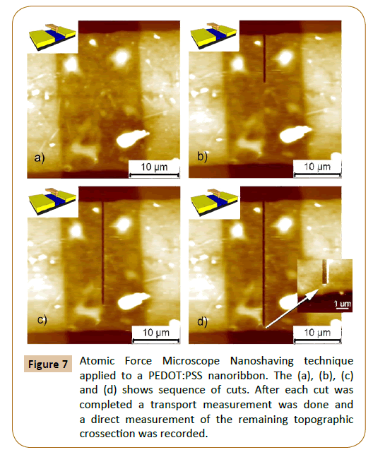
Figure 7: Atomic Force Microscope Nanoshaving technique applied to a PEDOT:PSS nanoribbon. The (a), (b), (c) and (d) shows sequence of cuts. After each cut was completed a transport measurement was done and a direct measurement of the remaining topographic crossection was recorded.
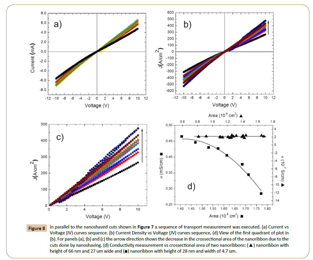
Figure 8: In parallel to the nanoshaved cuts shown in Figure 7 a sequence of transport measurement was executed. (a) Current vs Voltage (IV) curves sequence. (b) Current Density vs Voltage (JV) curves sequence, (d) View of the first quadrant of plot in (b). For panels (a), (b) and (c) the arrow direction shows the decrease in the crossectional area of the nanoribbon due to the cuts done by nanoshaving. (d) Conductivity measurement vs crossectional area of two nanoribbons: (▲) nanoribbon with height of 66 nm and 27 um wide and (■) nanoribbon with height of 28 nm and width of 4.7 um.
The nanoribbon shows a decrease in conductivity (■in Figure 8d) while area or conductivity increases. A reduction in the crosssectional area is effected by nanoshaving cuts in a unique behavior compared to the conductivity of PEDOT:PSS, which ranges from 10-3-103 S/cm [37-39]. The conductivity of this nanoribbon (Figures 4 and 7) shows a non-constant value and has a strong dependence on the nanoribbon’s cross-sectional area and it is observed a strong anisotropy in the conductivity dependence on the crossectional area. In order to make a comparison, we performed the same experiment on the nanoribbon of Figure 3, which has smaller dimensions than that of Figure 4. The nanoribbon of Figure 3 is 28 nm in height and 3.7 um in width. The nanoribbon was cut using nanoshaving methods described for the previous nanoribbon, and consequently the transport properties and (JV) curves were measured as a function of cuts or the remaining nanoribbon cross-sectional area. The resulting conductivity as a function of cross-sectional area is shown in Figure 8d as data point, and shows that the conductivity of the nanoribbon has a constant value as a function of area: classic conductivity behavior.
Conclusions
We have shown that PEDOT-PSS nanoribbons fabricated by electrospinning can produce two types of nanoribbons, which have a very low height on the order of 5 nm, and two different widths. It is possible for thin nanoribbons of PEDOTS-PSS for their height to be correlated to the reported crystal structure and orientation and reported nanocrystal dimensions of 4.8 nm for PEDOS-PSS [33]. AFM nanolithography methods were used to study the nanoribbon’s transport behavior. The transport properties do exhibit a non-classical behavior and strong anisotropic conductivity for nanoribbons of 66 nm height. For nanoribbons of 5 nm height, on the other hand, classical behavior is shown in the conductivity of the PEDOT-PPS.
Acknowledgments
We acknowledge contract grant sponsor: NSF; contract grant numbers: NSF-DMR-0923021, NSF-EPS-0701525, NSFEPS- 1002410; Contract grant sponsor: DoD; and contract grant numbers: W911NF-11-1-0184, W911NF-15-0049. This project as also partially supported by the Institute for Functional Nanomaterials (NSF Grant 1002410) and PR Space Grant (NASA Grant NNX15AI11H).
References
- Friend R (2006) Materials science: Polymers show they're metal. Nature 441: 37-37.
- Roldughin V, Vysotskii V (2000) Percolation properties of metal-filled polymer films, structure and mechanisms of conductivity. Progress in Organic Coatings 39: 81-100.
- Ohta T, Bostwick A, Seyller T, Horn K, Rotenberg E (2006) Controlling the electronic structure of bilayer graphene. Science 313: 951-954.
- Kallmann H, Pope M (1960) Bulk conductivity in organic crystals.
- Shirakawa H, Louis EJ, MacDiarmid AG, Chiang CK, Heeger AJ (1977) Synthesis of electrically conducting organic polymers: halogen derivatives of polyacetylene,(CH) x. Journal of the Chemical Society, Chemical Communications 16: 578-580.
- Gustafsson G, Cao Y, Treacy G, Klavetter F, Colaneri N, et al. (1992) Flexible light-emitting diodes made from soluble conducting polymers. Nature 357: 477-479.
- Carrasquillo KV, Pinto NJ (2012)TunableSchottky diodes fabricated from crossed electrospunSnO 2/PEDOT-PSSA nanoribbons. Materials Science and Engineering: B177: 805-809.
- Lu J, Pinto NJ, MacDiarmid AG (2002)Apparent dependence of conductivity of a conducting polymer on an electric field in a field effect transistor configuration. Journal of applied physics 92: 6033-6038.
- Martínez O, Bravo AG, Pinto NJ (2009) Fabrication of Poly(vinylidene fluoride-trifluoroethylene)/Poly (3,4-ethylenedioxythiophene)-polystyrene sulfonate composite nanofibers via electrospinning. Macromolecules 42: 7924-7929.
- Pinto NJ, Rivera D, Melendez A, Ramos I, Lim JH,et al. (2011) Electrical response of electrospun PEDOT-PSSA nanofibers to organic and inorganic gases. Sensors and Actuators B: Chemical 156: 849-853.
- Piner RD, Zhu J, Xu F, Hong S, Mirkin CA (1999) Dip-pen nanolithography. Science 283: 661-663.
- Rosa LG, Liang J (2009) Atomic force microscope nanolithography: dip-pen, nanoshaving, nanografting, tapping mode, electrochemical and thermal nanolithography. Journal of Physics-Condensed Matter 21 (48).
- Liang J, Rosa LG, Scoles G (2007)Nanostructuring, Imaging and molecular manipulation of dithiol monolayers on au(111) surfaces by atomic force Microscopy. Journal of Physical Chemistry C111: 17275-17284.
- Das A, Lei C, ElliottM, Macdonald JE, Turner M (2006) Non-lithographic fabrication of PEDOT nano-wires between fixed Au electrodes. Organic electronics 7: 181-187.
- DeFranco JA, Schmidt BS, Lipson M, Malliaras GG (2006) Photolithographic patterning of organic electronic materials. Organic Electronics 7: 22-28.
- Ouyang S, Xie Y, Wang D, Zhu D, Xu X, et al. (2014) Photolithographic patterning of highly conductive PEDOT: PSS and its application in organic lightâ€ÂÂÂÂemitting diodes. Journal of Polymer Science Part B: Polymer Physics 52: 1221-1226.
- Grigorescu A, Hagen C (2009)Resists for sub-20-nm electron beam lithography with a focus on HSQ: state of the art. Nanotechnology 20: 292001.
- Cui T, Liu Y, Chen B, Zhu M, Varahramyan K (2005) Printed polymeric passive RC filters and degradation characteristics. Solid-state electronics 49: 853-859.
- Khaldi A, Maziz A, Plesse C, Soyer C, Vidal F, et al. (2016) Synergetic PEDOT degradation during a reactive ion etching process. Sensors and Actuators B: Chemical 229: 635-645.
- Herzer N, Wienk MM, Schmit P, Spoelstra AB, Hendriks CE, et al. (2010) Fabrication of PEDOT–OTS-patterned ITO substrates. J. Mater. Chem. 20: 6618-6621.
- Santos L, Martin P, Ghilane J, Lacaze PC, Randriamahazaka H, et al.Electrosynthesis of well-organizednanoporous poly (3, 4-ethylenedioxythiophene) by nanosphere lithography. Electrochemistry Communications12: 872-875.
- Reano R, Kong Y, Low H, Tan L, Wang F, et al. (2004) Stability of functional polymers after plasticizer-assisted imprint lithography. Journal of Vacuum Science & Technology B 22: 3294-3299.
- Söderström K, Escarré J, Cubero O, Haug FJ, Perregaux S, et al. (2011) UVâ€ÂÂÂÂnanoâ€ÂÂÂÂimprint lithography technique for the replication of back reflectors for nâ€ÂÂÂÂiâ€ÂÂÂÂp thin film silicon solar cells. Progress in Photovoltaics: Research and Applications 19: 202-210.
- Bognár J, Szűcs J, Dorkó Z, Horváth V,Gyurcsányi RE (2013)Nanosphere Lithography as a Versatile Method to Generate Surfaceâ€ÂÂÂÂImprinted Polymer Films for Selective Protein Recognition. Advanced Functional Materials 23: 4703-4709.
- Yang Y, Lee K, Mielczarek K, Hu W, Zakhidov A (2011)Nanoimprint of dehydrated PEDOT: PSS for organic photovoltaics. Nanotechnology 22: 485301.
- Samitsu S, Iida T, Fujimori M, Heike S, Hashizume T, et al. (2005) Conductivity measurements of PEDOT nanowires on nanoelectrodes. Synthetic metals 152: 497-500.
- Amro NA, Xu S, Liu GY (2000) Patterning surfaces using tip-directed displacement and self-assembly. Langmuir 16: 3006-3009.
- Liu GY, Xu S, Qian Y (2000) Nanofabrication of self-assembled monolayers using scanning probe lithography. Accounts of chemical research 33: 457-466.
- Rosa LG, Jiang J, Lima OV, Xiao J, Utreras E, et al. (2009) Selective nanoshaving of self-assembled monolayers of 2-(4-pyridylethyl) triethoxysilane. Materials Letters63: 961-964.
- Okuzaki H, Harashina Y, YanH (2009)Highly conductive PEDOT/PSS microfibers fabricated by wet-spinning and dip-treatment in ethylene glycol. European Polymer Journal 45: 256-261.
- Martin DC, Wu J, Shaw CM, King Z, Spanninga SA, et al. (2010)The morphology of poly (3, 4-ethylenedioxythiophene). Polymer Reviews 50: 340-384.
- Aasmundtveit K, Samuelsen E,Pettersson L, Inganäs O, Johansson T, et al. (1999) Structure of thin films of poly (3, 4-ethylenedioxythiophene). Synthetic Metals 101: 561-564.
- Takano T, Masunaga H, Fujiwara A, Okuzaki H, Sasaki T (2012) PEDOT nanocrystal in highly conductive PEDOT: PSS polymer films. Macromolecules 45: 3859-3865.
- Kim EG, Brédas JL (2008) Electronic evolution of poly (3, 4-ethylenedioxythiophene)(PEDOT): From the isolated chain to the pristine and heavily doped crystals. Journal of the American Chemical Society 130: 16880-16889.
- Greczynski G, Kugler T, Keil M, Osikowicz W, Fahlman M, et al. (2001) Photoelectron spectroscopy of thin films of PEDOT–PSS conjugated polymer blend: a mini-review and some new results. Journal of Electron Spectroscopy and Related Phenomena 121: 1-17.
- Hwang J, Amy F, Kahn A (2006) Spectroscopic study on sputtered PEDOT• PSS: Role of surface PSS layer. Organic electronics 7: 387-396.
- Kim J, Jung J,Lee D, Joo J (2002) Enhancement of electrical conductivity of poly (3, 4-ethylenedioxythiophene)/poly (4-styrenesulfonate) by a change of solvents. Synthetic Metals 126: 311-316.
- Kim YH, Sachse C, Machala ML, May C, Müllerâ€ÂÂÂÂMeskamp L, et al. (2011) Highly conductive PEDOT: PSS electrode with optimized solvent and thermal postâ€Â treatment for ITOâ€ÂÂÂÂfree organic solar cells. Advanced Functional Materials 21: 1076-1081.
- Stöcker T, Köhler A, Moos R (2012)Why does the electrical conductivity in PEDOT: PSS decrease with PSS content? A study combining thermoelectric measurements with impedance spectroscopy. Journal of polymer science part B: polymer physics 50: 976-983.