Keywords
Activation energy; CdSe; Chemical route; HRTEM; Nanorod
Introduction
One dimensional (1D) nanorods, two dimensional (2D) nanofilms and three dimensional (3D) nanoparticles have been the subject of interest in recent years both in fundamental research and technological applications. Among them the synthesis of 1D nanorods and two dimensional (2D) nanofilms are very tricky, due to their efficient photovoltaic properties that have been demonstrated by the design of thin films consisting of crystalline arrays of oriented nanorods. Nanorods exhibits substantial photocurrent efficiencies due to better transport and the photo-generated electrons are collected through a designed path (i.e., the oriented rods), as well as to a better physical and structural match between the n-type semiconductor materials, the diameter of its nanometer scale building blocks, and the minority carrier (hole) diffusion length. Such properties differ significantly from others, making nanorods potential candidates for integration into functional materials such as optoelectronic devices and biosensors [1-3]. For practical applications, nanorods provide the basis to the engineering of new materials and the fabrication of devices. In particular, embedding quantum structures in single nanorods would enable novel physical properties such as quantum confinement to be exploited, for example, the continuous tuning of spectral wavelength by varying the well thickness. 1D semiconductor nanostructures have been the subject of numerous research activities [4-7] and have been used to realize prototype electrical [8,9] and optical [10,11] test beds. Recently the preparations of nanorods and nanowires with axially and radially modulated compositions have been fabricated by various methods [12-17]. Inorganic nanorods have a strong tendency to aggregate in the solid state, and CdSe nanorods have been shown to exhibit liquid crystal phases in concentrated solutions, or when cast from solution onto a substrate [18-21]. CdSe nanorods also show gross phase separation when blended with most polymers as composite films [11,22]. CdSe nanorods with narrow size distribution are also readily available because of recent synthetic advances [23,24].
The structural and optical properties of CdSe nanorods have been studied by many researchers but no attention has ever been paid for a systematic study of the dielectric relaxation of CdSe nanorods. In the present work we have focused in a comparative dielectric study of CdSe nanoparticles [25] with CdSe nanorods and it actually explains the advantage of CdSe nanorods as the long axis of the nanorods provides a continuous pathway for electron transport for nanorods.
Experimental Techniques
In the synthesis of the materials, the precursors used were cadmium acetate [(CH3COO) 2Cd, 2H2O), Merck] and sodium selenite (Na2SeO3, 5H2O), Loba chemie). Mercapto ethanol ((C2H6OS), SRL) was used as the capping agent.
A detailed study of the preparation of CdSe nanorods have been discussed in our previous publication [26] where the phase formation of the material is checked by the X-ray diffraction (XRD) pattern. The XRD pattern of the materials [26] clearly indicates that there is no mixed phase in the materials. The size of the nanoparticles is determined by the transmission electron microscope ((TEM) which has already been reported in our earlier work) [26]. A detailed study of the structural, optical and vibrational properties of the CdSe nanorods has been published in our previous publication [26].
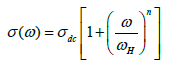
For the dielectric measurement, the powder of CdSe was pelletized into a disc of thickness 2.9 mm and diameter 8.01 mm using a pressure of 4 tons. The disc was gold electroded and connected to an LCR meter (Hioki - 3552). The frequency dependence of dielectric parameters was measured in the various frequency ranges (from 1000 Hz to 1.1 MHz) over a different temperature range (from 323 to 473 K). The temperature was controlled by a programmable temperature controller (Eurotherm 2216e) connected with the oven. All the dielectric data were collected at a rate of 1°C /min while heating or cooling. Each measured temperature was kept constant with an accuracy of 1°C. The three important parameters like complex electric modulus M* (=1/ ε*) and complex impedance Z* (=M*/ jωCo) and ac electrical conductivity (ω)=ωεoε″ were obtained from the temperature dependence of the real (ε′) and imaginary (ε″) components of the dielectric permittivity ε* (= ε′ - j ε″).
Results and Discussion
Impedance Spectroscopy analysis
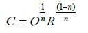
Impedance formalism: Figure 1 shows the complex impedance plane plots of CdSe nanorods at different temperatures. In the impedance formalism, there are three contribution arises from grain, grain-boundary and specimen-electrode interface effect in the relaxation process. A circular/semicircular arc gives rise to each of these contributions in the Cole-Cole model where the grain effect is occurred in the higher frequency arc, midfrequency arc represents the grain-boundary effect and lower frequency arc is attributed to the electrode effect [27,28]. There are two types of relaxation phenomena signifying two different arcs in the impedance plane plots at each temperature with sufficiently different relaxation times (τ=RC), where R is the resistance and C is the capacitance of the associated phase [29]. Polycrystalline materials generally show intergranular or grain-boundary impedances. The impedance data is modelled by invoking an equivalent circuit consisting of two serially connected R-CPE units, for the grain and grain boundary region, each containing a resistor (R) and a constant phase element (CPE) (instead of ideal capacitor) in parallel. In the inset of the Figure 1, an equivalent circuit model (RgQg) (RgbQgb) is shown to interpret the impedance plane plots. Here R, Q, g, gb represent the resistance, the constant phase element, grain elements and grain boundaries, respectively. The CPE is used to accommodate the non-ideal behaviour of the capacitance which may have its origin in the presence of more than one relaxation process with similar relaxation times. The capacitance of the CPE is given by the following relation
 (1)
(1)
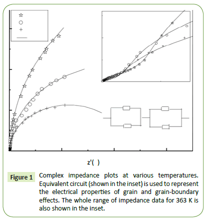
Figure 1: Complex impedance plots at various temperatures. Equivalent circuit (shown in the inset) is used to represent the electrical properties of grain and grain-boundary effects. The whole range of impedance data for 363 K is also shown in the inset.
where the non-ideal behaviour is estimated by the parameter n, having a value of zero for pure resistive behaviour and is unity for capacitative behaviour [30-32]. In the complex plane plot, the arc representing the grain boundaries generally lies on the lower frequency side since the relaxation time of the grain boundaries is much larger than that of the grains [33]. Therefore, we assign smaller (high frequency) and larger (low frequency) semicircular arcs to the grain and grain boundary, respectively [34]. The parameters Rg, Rgb, Qg, Qgb, ng, and ngb are obtained for each temperature by fitting the impedance plane plots. The fitting parameters derived from the equivalent circuit are given in Table 1.
| Temp (K) |
Rg (ohm) |
Qg (ohm-1 m-2 S-n) |
ng |
Rgb (ohm) |
Qgb (ohm-1 m-2 S-n) |
ngb |
| 373 |
3.85 104 |
6.1 10-9 |
0.7 |
2.5 107 |
1 10-9 |
0.55 |
| 403 |
1.8 104 |
6 10-9 |
0.69 |
7.5 106 |
0.9 10-9 |
0.62 |
| 443 |
0.85 104 |
5.5 10-9 |
0.68 |
4.5 106 |
0.85 10-9 |
0.63 |
Table 1: Complex impedance plane fitting parameters based on the R-CPE equivalent circuit.
As evidenced from Table 1, the value of ng decreases and ngb increases with an increase in temperature signifying that the grain boundary capacitance (Cgb) is likely to approach ideal behaviour and the grain capacitance (Cg) deviates from the ideal behaviour. The variation in the resistances of the grain and grain boundaries with temperature is also enlisted in Table 1. The decrease in the resistance of grains and grain boundaries may be due to the thermal activation of the localized charges. Two types of thermal activation processes one is carrier density in the case of band conduction and the other one is carrier mobility in case of hopping, are responsible for the reduction in the resistive properties with temperature [35].
Dielectric relaxation
Figure 2 shows the plot of real (ε′) and imaginary (ε″) parts of the complex permittivity for CdSe as a function of logarithmic angular frequency ω (= 2πν) at various temperatures. The value of ε′ decreases with increasing frequency and becomes almost independent of frequency after a certain value observed in Figure 2a. We may discuss it in a different way: at very low frequencies (when ω<<1/τ, where τ is the relaxation time), dipoles can follow the field and ε′ is nearly equal to its value at quasi-static fields. With the increase of frequency (when ω<1/τ), dipoles begin to lag behind the field and ε′ slightly decreases and finally at the characteristic frequency (ω=1/τ), the dielectric constant drops and shows the relaxation process. At very high frequencies (when ω >>1/τ), dipoles can no longer follow the field and ε′ reaches its high-frequency value.
Figure 2: Frequency (angular) dependence of ε′ (a) and ε" (b) of CdSe nanorods at various temperatures, where the symbols represent the experimental data and the solid lines are the Cole–Cole fits to the experimental data using Eqs. (4) and (5).
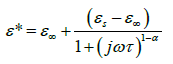
In Figure 2b, a relaxation peak is developed in the logarithmic angular frequency dependence of ε″ in the dispersion region of ε′. The peak position in the frequency dependence of ε″ shifts to the higher-frequency side with increasing temperature where the increase in the value of ε″ in the low-frequency region is due to the dc conductivity. It is clear that the width of the loss peaks in Figure 2b points towards the possibility of a distribution of relaxation times. Cole– Cole model is one of the most convenient ways of checking the poly-dispersive nature of the dielectric relaxation where the complex dielectric constant is known to be described by the empirical relation [36].
 (2)
(2)
where εs − ε∞ is the dielectric strength, τ is the mean relaxation time, and α is the Cole–Cole parameter which varies between 0 and 1. For an ideal Debye relaxation α=0, and α > 0 signifies that the relaxation has a distribution of relaxation times, which gives a broader peak shape than a Debye peak. In some cases, when the electrical conductivity is dominant in the low-frequency range a contribution term by electrical conduction is generally added to the relaxation equation. The the conductivity term is incorporating in the modified Cole–Cole equation given as [37,38].
 (3)
(3)
Where σ* (= σ1+jσ2) is the complex conductivity followed by the real and imaginary part. From the above relation, the complex permittivity can be decomposed into the real and imaginary parts
 (4)
(4)
and
 (5)
(5)
where the free charge carriers (dc conductivity) and the space charge carriers (localized charges) are represented by σ1 and σ2 and n is a dimensionless frequency exponent which varies from 0 to 1. It is evident from the above equations that the charge carrier localization at the interfaces (to the dielectric loss. In Equation (5), the first term indicates the part of the losses associated with the dielectric σ2) can make a large contribution to the dielectric permittivity, whereas the free charge carriers (σ1) contribute relaxation due to permanent dipole orientation, whereas the second term explains the losses associated with long-range migration of the charge carrier response. We have analyzed our experimental data using Equation (4) and (5) and the best fitting of the experimental data is shown by solid lines in Figures 2a and 2b. The obtained fitting parameters are listed in Table 2. It is observed that with increasing temperature, the value of n increases. Here, the exponent n represents the degree of interaction between mobile charges with the lattice around them and n=1 for an ideal complex conductivity (where the interaction between the neighboring dipoles is almost negligible). For n<1 the polarization has a distribution of the carrier polarization mechanism. The mobile charge carriers easily escape the potential barriers at a particular frequency with increasing temperature and hence the interaction with the lattice sites decreases giving the higher value of n for the system. In the low-temperature region the electric dipoles formed by the mobile charge carriers freeze easily through the relaxation process at lower frequency due to the high interaction with lattice sites. So, Figure 2a indicates a strong dispersive nature of the carrier polarization mechanism by decay of polarization with respect to the applied field. On the other hand, at high temperatures the polarization of charge carriers occurs quickly and thus the relaxation occurs on the high-frequency side, indicating the weakly dispersive nature of carrier polarization [39,40]. To get an idea about the type of relaxation response in this material, we have calculated the activation energy of the relaxation process. To obtain the required activation energy for the dielectric relaxation process, we have plotted the characteristic relaxation frequency (ωm) as a function of temperature, shown in Figure 3 which satisfies the Arrhenius law and the activation energy is found to be ~ 0.391 eV. Such a value of activation energy indicates that the conduction mechanism in CdSe may be due to polaron hopping based on the electron carriers [41,42]. In the hopping process, the electron disorders its surroundings by moving its neighboring atoms from their equilibrium positions and forms the polaron.
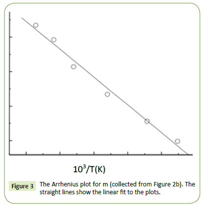
Figure 3: The Arrhenius plot for m (collected from Figure 2b). The straight lines show the linear fit to the plots.
| T (°K) |
Δε =(εs- ε∞) |
α |
n |
ωmax (106 rad s-1) |
σ1 (10-6 S m-1) |
σ2 (10-6 S m-1) |
| 373 |
78 |
0.15 |
0.89 |
0.45 |
2.1 |
1.7 |
| 403 |
80 |
0.13 |
0. 90 |
1.1 |
3.1 |
4.2 |
| 423 |
81 |
0.12 |
0.91 |
2.55 |
4.5 |
- |
| 473 |
82 |
0.11 |
0.93 |
7 |
10.7 |
9.5 |
Table 2 : The fitting parameters for ε′ and ε".
Presence of amorphous phase at nanorod interface is confirmed from HRTEM analysis. Nanorods cress-cross each other when they are subjected to high pressure to form a pellet. Finally this phase percolate for electrical conduction and treated as grain boundary with the nanorod itself acting as grain. In CdSe nanorods as the band gap is smaller than that of CdSe nanoparticles, the defect states have to be distributed with narrower energy range. Reduction of grain boundary activation energy of ~ 0.39 eV in nanorods from ~ 0.8 eV in nanoparticles supports this statement.
Figure 4 shows the scaling behaviour of ε″ where we have scaled each ε″ by εm″ (εm″ is the peak value of ε″ in the ε″ vs logω plot) and each frequency by ωm (corresponds to the frequency of the peak position of ε″ in the ε″ vs log ω plot). From Figure 4 it can be said that the relaxation describes the same mechanism at different temperatures in this material as all the curves superimposed in a single master curve for all the temperatures.
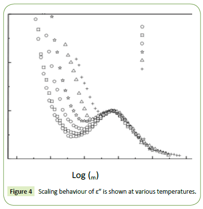
Figure 4: Scaling behaviour of ε" is shown at various temperatures.
Conductivity formalism
The conductivity of the sample can be measured by the given expression as
σ (ω) =ωεoε " (6)
where is the real part of the conductivity and ε" is the imaginary part of dielectric constant. Figure 5a shows the frequency spectra (log-log plot) of the conductivity for CdSe nanorods at different temperatures.
As illustrated in Figure 5b, a typical conductivity spectrum at 403 K is divided into three different parts [43]. In region I, the jump relaxation model (at low frequency and/or at high temperature, since the electric field cannot perturb the hopping conduction mechanism of charged particles), explains the conductivity is approximately equal to the dc value and the conduction mechanism is the same as that for dc conduction, i.e., hopping of charged particles from one localized state to another. This localization gives rise to the formation of the polaron and the charge transport may be considered between the nearest neighbour sites. In region II, the conductivity begins to increase nonlinearly after the frequency exceeds the critical frequency ωc it may be due to the fact that the capacitor admittance becomes numerically larger than the resistor admittance with increasing frequency. Now the conductivity becomes proportional to frequency in region III and produced nearly constant loss (NCL). Thus it is observed that the ac conductivity at high frequency is dominated by the NCL regime in CdSe nanorods. It is seen from Figure 5a that with decreasing frequency the value of σ decreases and after a certain value, it becomes independent of frequency. Extrapolation of this part towards lower frequency will give σdc value of the particulars. At higher frequency σ exhibits dispersion, increasing in a power law fashion and eventually becoming almost linear. Thus the conductivity spectra are analyzed by the power law shown in Figure 5c [44,45] given by
 (7)
(7)
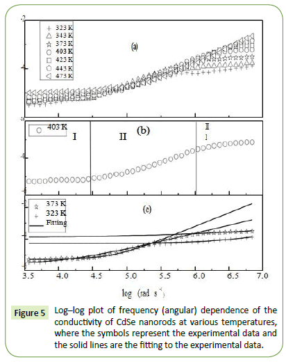
Figure 5: Log–log plot of frequency (angular) dependence of the conductivity of CdSe nanorods at various temperatures, where the symbols represent the experimental data and the solid lines are the fitting to the experimental data.
Where σdc is the DC conductivity, ωH is the hopping frequency of the charge carriers and n is a dimensionless frequency exponent. In lower frequency region the value of n varies in the range of 1 ≤ n ≤ 2 whereas in the high frequency region it is found to be in the range of 0-1. At low frequency, the ac conductivity is found to be weakly frequency dependent due to the non-equilibrium occupancy of the trapped charges [46]. With increasing frequency, the occupancy of the trap centers is reduced for conduction process which facilitates the conductivity state more active by promoting the hopping of electrons and holes. As a result, with increasing frequency and temperature, the conductivity increases. The experimental conductivity spectra of CdSe nanorods are fitted to Equation 7 with σdc and ωH as variable and the parameter n is weakly temperature dependent.
A comparison of the values of conductivity of CdSe nanorods with CdSe nanoparticles at a particular frequency (1 MHz) for different temperatures is given in Table 3.
| Temp. (K) |
CdSe nanorods σdc X 10-6(S m-1) |
CdSe nanoparticles σdc X 10-6 (S m-1) |
| 443 |
650 |
631 |
| 403 |
308 |
224 |
| 343 |
144 |
91 |
| 323 |
69 |
50 |
Table 3 : Comparison of conductivity values of CdSe nanorods and CdSe nanoparticles.
Conclusion
We have synthesized CdSe nanorods by soft chemical route. It is cubic in phase and rod like shaped, confirmed from XRD and TEM images. The dielectric relaxation mechanism of the sample is carried out by impedance spectroscopy analysis. Relaxation peaks are observed in the imaginary part of the complex permittivity spectra and is fitted by the modified Cole-Cole expression. Grain and grain boundary effects both are present in the complex impedance plane plot and is analyzed by an electrical equivalent circuit consisting of a resistance and a constant-phase element (CPE). There are two plateaus in the frequency-dependent conductivity spectra which explain the presence of both the grain and grain boundary contribution in conductivity analysis.
References
- Duan XF, Huang Y, Cui Y, Wang J, Lieber CM (2001) Indium phosphide nanowires as building blocks for nanoscale electronic and optoelectronic devices. Nature 409: 66-69.
- Johnson JC, Choi HJ, Knutsen KP, Schaller RD, Yang PD, et al. (2002) Single gallium nitride nanowire lasers. Nat Mater 1: 106-110.
- Xia YN, Yang PD, Sun YG, Wu YY, Mayer B, et al. (2003) One-dimensional nanostructures: Synthesis, characterization and applications. Adv Mater 15: 353.
- Hu JT, Odom TW, Lieber CM (1999) Chemistry and physics in one dimension: Synthesis and properties of nanowires and nanotubes. Acc Chem Res 32: 435-445.
- Pan ZW, Dai ZR, Wang ZL (2001) Nanobelts of semiconducting oxides. Science 291: 1947-1949.
- Wang ZL (2003) Nanowires and Nanobelts. Kluwer Academic Publisher, New York, USA.
- Morales AM, Lieber CM (1998) A laser ablation method for the synthesis of crystalline semiconductor nanowires. Science 279: 208-211.
- Huang Y, Duan XF, Cui Y, Lauhon LJ, Kim KH, et al. (2006) Logic gates and computation from assembled nanowire building blocks. Science 294: 1313-1317.
- Goldberg J, Hochbaum AI, Fan R, Yang PD (2006) Silicon Vertically Integrated Nanowire Field Effect Transistors. Nano Lett 6: 973-977.
- Kazes M, Lewis DY, Ebenstein Y, Mokari T, Banin U (2002) Lasing from semiconductor quantum rods in a cylindrical microcavity. Adv Mater 14: 317.
- Huynh WU, Dittmer JJ, Alivisatos AP (2002) Hybrid nanorod-polymer solar cells. Science 295: 2425-2427.
- Ding X, Huang Y (2017) Synthesis of silver nanowire and preparation of uniform, highly conductive transparent films on flexible substrate with extremely excellent film performance. J Nanosci Nanotech 17: 705-710.
- Jia Q (2011) Hydrothermal synthesis of one-dimensional single-crystalline rutile TiO2 nanostructures and their application in dye-sensitized solar cells. J Nanosci Nanotech 11: 9846-9850.
- You S, Park SY, Choi HW, Kim KH (2015) Properties of silver nanowire/zinc oxide transparent bilayer thin films for optoelectronic applications. J Nanosci Nanotech 15: 8656-8661.
- Choo DC, Lee JG, Tae W (2015) Transparent conducting silver-nanowire-embedded poly(methyl methacrylate) nanocomposite films formed by using a transfer method. J Nanosci Nanotech 15: 7598-7601.
- Hui KN, Yin C, Hui KS, Lee JY, Li M, et al. (2012) Synthesis of Co3O4 nanowire arrays supported on Ni foam for removal of volatile organic compounds. J Nanosci Nanotech 12: 3563-3566.
- Xie H, Xiong HN, Wang YH, Zhao YZ, Li JZ, et al. (2016) Sintering behavior and effect of silver nanowires on the electrical conductivity of electrically conductive adhesives. J Nanosci Nanotech 16: 1125-1137.
- Querner C, Benedetto A, Demadrille R, Rannou P, Reiss P (2006) Carbodithioate-containing oligo- and polythiophenes for nanocrystals' surface functionalization. Chem Mater 18: 4817-4826.
- Kim F, Kwan S, Akana J, Yang PD (2001) Langmuir−Blodgett nanorod assembly. J Am Chem Soc 123: 4360-4361.
- Li LS, Alivisatos AP (2003) Semi-conductor nanorod liquid crystals and their assembly on a substrate. Adv Mater 15: 408.
- Li LS, Walda J, Manna L, Alivisatos AP (2002) Semi-conductor nanorod liquid crystals. Nano Lett 2: 557-560.
- Zhang Q, Gupta S, Emrick T, Russell TP (2006) Surface-functionalized CdSe nanorods for assembly in diblock copolymer templates. J Am Chem Soc 128: 3898-3899.
- Peng XG, Manna L, Yang WD, Wickham J, Scher E, et al. (2000) Shape control of CdSe nanocrystals. Nature 404: 59-61.
- Peng ZA, Peng XG (2002) Nearly monodisperse and shape-controlled CdSe nanocrystals via alternative routes: Nucleation and growth. J Am Chem Soc 124: 3343-3353.
- Das S, Dutta A, Ghosh B, Banerjee S, Sinha TP (2014) Dielectric relaxation of CdSe nanoparticles. J Phys Chem Sol 75: 1245.
- Das S, Dutta A, Banerjee S, Sinha TP (2015) Dielectric relaxation of CdO nanoparticles. Mat Sci Semiconductor Process 40: 412.
- Das S, Banerjee S, Sinha TP, Dutta A (2014) Phonon modes and activation energy of Fe-doped CdSe nanoparticles. Physica E 78: 73.
- Tripathi R, Dutta A, Das A, Sinha TP (2015) Dielectric relaxation of CdO nanoparticles. Appl Nanosci 6: 175.
- Nadeem M, Akhtar MJ, Haque MN (2008) Increase of grain boundary resistance with time by impedance spectroscopy in LaO.50CaO.50MnO3+δ at 77 K. Solid State Commun 145: 263-266.
- Nadeem M, Afzal AB, Akhtar MJ, Nadeem M, Hassan MM (2009) Investigation of structural and electrical properties of polyaniline/gold nanocomposites. J Phy Chem C 113: 17560-17565.
- Chandran A, Samuel MS, Koshy J, George KC (2011) Dielectric relaxation behavior of CdS nanoparticles and nanowires. J Mater Sci 46: 4646.
- Ross J, Macdonald N (1987) Impedance spectroscopy: Theory, experiment, and applications. (2nd edn). Wiley, New York.
- Iguchi E, Nakamura N, Aoki A (1997) Electrical transport properties in semiconducting BaPbxBi1 − xO3 using complex-plane impedance analyses. J Phys Chem. Solids 58: 755-763.
- Idrees M, Nadeem M, Hassan MM (2010) Investigation of conduction and relaxation phenomena in LaFe0.9Ni0.1O3by impedance spectroscopy. J Phys D 43: 155401.
- Gerhardt R (1994) Impedance and dielectric spectroscopy revisited: Distinguishing localized relaxation from long-range conductivity. J Phys Chem Solids 55: 1491-1506.
- Cole KS, Cole RH (1941) Dispersion and absorption in dielectrics I. Alternating current characteristics. J Chem Phys 9: 341-351.
- Thongbai P, Tangwancharoen S, Yamwong T, Maensiri S (2008) Dielectric relaxation and dielectric response mechanism in (Li, Ti)-doped NiO ceramics. J Phys Condens Matter 20: 395227.
- Ming D, Reau JM, Ravez J, Gitae J, Hagenmuller P (1995) Impedance-spectroscopy analysis of a LiTaO3-type single crystal. J Solid State Chem 116: 185-192.
- Karthik C, Varma KBR (2006) Dielectric and AC conductivity behavior of BaBi2Nb2O9 ceramics. J Phys Chem Solids 67: 2437-2441.
- Lin Y, Jiang L, Zhao R, Nan CW (2005) High-permittivity core/shell stuctured NiO-based ceramics and their dielectric response mechanism. Phys Rev B 72: 014103.
- Iguchi E, Ueda K, Jung WH (1996) Conduction in LaCoO3 by small-polaron hopping below room temperature. Phys Rev B 54: 17431-17437.
- Komine S, Iguchi E (2007) Dielectric properties. J Phys Chem Solids 68: 1504-1507.
- Li W, Schwartz RW (2006) AC conductivity relaxation processes in CaCu3Ti4O12 ceramics: Grain boundary and domain boundary effects. Appl Phys Lett 89: 242906.
- Jonscher AK (1983) Dielectric relaxation in solids. Chesla Dielectric Press, London.
- Hairetdinov EF, Uvarov NF, Patel HK, Martin SW (1994) Estimation of the free-charge-carrier concentration in fast-ion conducting Na2S-B2S3 glasses from an analysis of the frequency-dependent conductivity. Phys Rev B 50: 13259-13266.
- Nandeem M, Mushataq A (2009) Thermal cycling induced reversibility/irreversibility in the ac electrical properties of LaO.50CaO.50MnO3+δ by impedance spectroscopy. J Appl Phys 106: 073713.