Research Article - (2023) Volume 7, Issue 2
A Semi-empirical Approach to Bulk Modulus of ANB8-N Semiconductors and Their Alloys
Mritunjai Kumar Pathak1,
Madhu Sudan Dutta1,
Sanjay Kumar Gorai2,
Ashok Kumar Gupta1,
Rajendra Nath Sinha1 and
Parmanand Mahto1*
1Department of Physics, Vinoba Bhave University, Hazaribag, Jharkhand, India
2Department of Physics, Tata College, West Singhbhum, Jharkhand, India
*Correspondence:
Parmanand Mahto, Department of Physics, Vinoba Bhave University, Hazaribag, Jharkhand,
India,
Tel: pmahtovbu@rediffmail.com,
Received: 21-Feb-2023, Manuscript No. IPACRH-23-15742;
Editor assigned: 23-Feb-2023, Pre QC No. IPACRH-23-15742 (PQ);
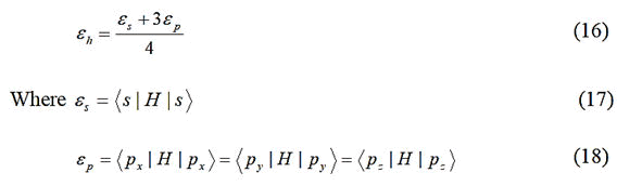
Reviewed: 09-Mar-2023, QC No. IPACRH-23-15742;
Revised: 21-Apr-2023, Manuscript No. IPACRH-23-15742 (R);
Published:
28-Apr-2023, DOI: 10.21767/2572-4657.23.7.11
Abstract
In this study, a semi-empirical relation has been developed for bulk modulus in terms of bond energy
and bond length and applied to elemental and binary semiconductors. The basis of this formula
originates from the very definition of bulk modulus. The universal parameter tight binding approach
has been utilized with some modification in the overlap parameter to evaluate bond energy and bond
length. The results are in reasonable agreement with those of experiments. The new formula has also
been applied to ternary as well as quaternary alloys of II-VI and III-V semiconductors including some
highly mismatched alloys. The trend of variation of bulk modulus with composition for both cationic
and anionic substitution is explained in terms of ionic size effect.
Keywords
Bond energy; Bond length; Bulk modulus; Solar cell; Highly mismatched alloys; Universal
parameter tight binding theory
Introduction
Semiconductors have long been used widely in electronic
industry and today there is hardly any field left without the
application of semiconductors. This is because each type of
semiconductors has some specific characteristics for an
application. The range and horizon of application of
semiconductors is broadened further by allowing them to
tailor the material properties like lattice parameters, band
gaps, bond length, iconicity hardness, bulk modulus etc.
required for the new and desired applications [1-13]. For
example, the dilute nitride alloys GaAs1-xNx and Ga1-xInxAs1-yNy; dilute oxide alloys ZnS1-xOx and Zn1-xCdxTe1-yOy and some other such combinations BxGa1-xN, ZnO1-xTex have been identified as Highly Mismatched Alloys (HMAs)
which are the potential candidates for high efficiency solar
cell. However, the stability of solar cells is of concern for their
application in space, where they have to withstand
bombardment of high energy particles like electrons, protons
cosmic rays etc. that can cause severe damage to solar cells.
Also in domestic, industrial and commercial applications the
electronic appliances have to face mechanical stresses and
electrical jerks due to voltage fluctuations.
Therefore, study on mechanical properties of these
semiconductors and their alloys are of prime importance.
Among these properties, focus has been made on bulk
modulus, which has in many cases been correlated with
material strength and hardness, and it is commonly accepted that material with larger bulk modulus are accepted to be
harder ones. Of course, this is not always true and recently it
has been found that even the materials with very high bulk
moduli have low hardness. For example, Rhenium was
predicted to have high bulk modulus (405 GPa), but its
(Vickers’s) hardness was found to be 16.7 GPa, which is about
five times lower than that of diamond [14]. Based on this
common concept, C3N4 was initially proposed to be one of the
hardest materials comparable with diamond as its bulk
modulus was estimated to be 443 GP, but later on it was
synthesized and its hardness was found to be even lower than
diamond and BN [15]. Even then bulk modulus is considered
as one of the important parameters to characterize physical
properties, and for many applications it is used as indicator
for materials strength and hardness. In the backdrop of the
above scenario, a semi-empirical formula has been developed
and presented in this study for bulk modulus of Group IV and
IV-IV, II-VI and III-V semiconductors and their ternary and
quaternary alloys.
Materials and Methods
Theoretical Methods
Brief review of earlier researches: On the theoretical front
empirical tight binding method [16], effective bond orbital
method [17,18], empirical self-consistent pseudopotential
method [19] and density functional theory [20] have emerged
as powerful tools for precise calculation of ground state
properties of materials. Although various software is,
available for these methods, they require profound
understanding of the nature of chemical bonding in materials
and also advanced computational facilities. Empirical
methods easy to work and they also produced results quite in
agreement with experimental values and also with those
obtained from the advanced computational schemes.
Therefore, a number of empirical methods have been
developed by researchers for computing bulk modulus of
semiconductors. Cohen developed the following bond length
(d in Å) dependent relation for bulk modulus of
semiconductors.
B=1761d-3.5 (1)
Where;
B=Bulk modulus.
Later on an empirical parameter, λ was introduced in this
formula to incorporate the effect of iconicity which stands as
follows,
B=(1971-220 λ )/d3.5 (2)
Where;
λ=0,1 and 2 for group-IV and IV-IV, III-V and II-Vi respectively.
This formula was quite successful in estimating bulk modulus
of III-V semiconductors, but a deviation of estimated values
from experimental ones resulted in the range 10.1%-17.3% in
case of II-VI systems. This relation was further extended to study non-octet semiconductors like Si3N4 for which following
modified formula was suggested.
B=<NC>(1971-220 λ )/4d3.5 (3)
Where;
<NC>=Stands for an average coordination number.
Lam, et al., however, deduced an analytical relation of bulk
modulus to the lattice parameters within the local
density approximation and the pseudopotential as:
B=(1971/d3.5)–408 (ΔZ)2/d4 (4)
Where;
ΔZ=0,1,2,3 for group-IV, III-V, II-VI and I-VII semiconductors
respectively. But this formula was applicable to III-V
semiconductors only. For II-VI systems they suggested some
modification in it. Al-Douri, et al., also suggested a formula
similar to that of Cohen.
B=(3000-100 λ) (a/2)-3.5 (5)
Where;
a=Lattice parameter. This formula estimated the values of
bulk modulus which are consistent with the experimental
results.
Neumann proposed a formula of bulk modulus in terms of
lattice parameter ‘a’ and spectroscopically defined bond
iconicity, fi figured as:
B=boa-m(1-gofi) (6)
Where;
bo, m and go are constants and have the same value for all
compounds. Al-Douri further proposed two formulae as:
B=(60- λ20). (EgΓX/αm) (7)
B=(30+ λ10) ((Pt1/2/ EgΓX)/3) (8)
Where;
αm=Metallicity (in eV); EgΓX=Energy gap (in eV) along Γ–X. λ=0,
2 and 2.65 for group IV, III-V and II-VI semiconductors
respectively.
Pt=Transition pressure.
Kamran, et al., however, suggested and also attempted to give
theoretical basis to the following formula of bulk modulus:
B=(1938.72-506.702 fi)/d3.5 (9)
Where;
fi=Bond iconicity.
Results obtained using this formula, in general, fall within 19%
of the experimental values. In the bond orbital method
however, the bulk modulus was proposed as:
B=2*31/2(V2 αc3 + 7.8/d2)/3d3 (10)
Where;
V2=Covalent energy, is given by,
V2=-ηħ2/4π2md2 (11 )
Here;
η=Overlap parameter,
αc=Covalence of the bond and m is the mass of the electron.
This formula could give somewhat better results. In the ionic
charge approach of bond orbital model, Verma proposed a d-3
dependence formula of bulk modulus.
A new formula proposed: Various formulae noted in the
above sub-section clearly demonstrated the bond length
dependence of bulk modulus along with some other
parameters like bond ionicity, band gap, covalency, transition
pressure, metallicity, covalent energy, bond charge etc. But
the values predicted with different formulae differ widely
among themselves and from the experimental ones. Also, the
d-dependence power varies like d-3.5, d-4 and d3. This aspect,
therefore, needs to be revisited. In this attempt, we begin
with the basic definition of bulk modulus and proposed a semi
empirical formula. From definition, bulk modulus, the
property of a material showing its resistance to volume
change on compression, is given by
B=-P/(dV/V) (12)
Where;
dV/V=Volume strain is dimensionless and the stress
P=F/A=E/V (13)
Here;
F=Force (restoring),
A=Area,
E=Energy
V=Volume.
The volume of the unit cell of a cubic crystal, V ∝ d3.
Where;
d=Bond length.
Therefore, bulk modulus should bear an inverse cubic
dependence relation with bond length, i.e.
B ∝ E/d3 (14)
Here, bond energy Eb is proposed to be used in place of E.
This is because the bond energy of a stronger bond must be
higher and for such a bond the resistance against any
deformation (volume) should be higher giving rise to higher
bulk modulus. Accordingly, B is expected to bear a linear
relationship with Eb/d3. With this assumption, we have
applied the Universal Parameter Tight Binding (UPTB) theory
to evaluate Eb and d for group–IV, IV-IV, III-V and II-VI
semiconductors and some ternary and quaternary alloys.
Then graphs were plotted for B versus Eb/d3 for group-IV and
IV-IV, III-V and II-VI systems which were found to be linear,
with the help of which the new relation has been proposed.
But before arriving at the new relation, a brief introduction of
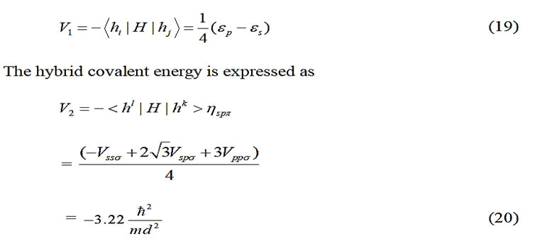
UPTB theory appears plausible. In the UPTB formalism, the bond energy is expressed in terms of four main contributing
energy terms as:

Where;
Ep=Promotional energy.
Eσ=Sigma bond formation energy.
Eo=Overlap energy.
Em=Metallization energy.
These constituent energies are expressed in parameterized
forms through the metallic, covalent, polar and hybrid
energies, which are expressed in terms of atomic orbital
energies. Actually, the metallic, covalent, polar and hybrid
energies originate out of the non-zero matrix elements of the
Hamiltonian between hybrids of the bond forming atoms.
The hybrid energy (expectation value) of a tetrahedral solid
having sp3 hybrids is given by
H=Hamiltonian of the system.
These energy values differ somewhat in the solids from the
corresponding values for free atoms. However, following
Harrison’s prescription the free atom energy (Hartree-Fock
term) values have been utilized in the present work. The
metallic energy is given by
For tetrahedral solids, considering matrix elements between
nearest neighbor atoms only, Froyen and Harrison proposed
that;
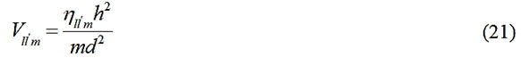
Where;
where the subscript m is a quantum number, but m in the
denominator represents the electron mass, d is the bond
length (in Å ) ηll'm and is a dimensionless coefficient with

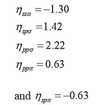
In case of polar covalent solids, the hybrid polar energy is
represented as:
Where;
c(a)=Cation (anion).
Therefore, following kraut and Harrison, a general expression
of bond energy as given below was utilized.
Where;
V1IV(c) and V1IV(a) are the values of V1 for the column-IV
elements from the rows of the atoms corresponding to the
cation and the anion respectively. In the equilibrium state, the
bond energy is minimum. But among the various energy
terms, only V2 includes ‘d’. So Eb was minimized with respect
to V2. Then employing Newton-Raphson numerical technique,
the self-consistent values of V2, d and Eb were obtained. For
selection of the overlap parameter ηo, initially, Harrison’s
approach of using geometrical mean of ηo values
corresponding to the respective homoploid semiconductor,
i.e. for a compound AiBj with i and j denoting rows of elements
A and B in the periodic table, tehffee ctive ηo is given by:
Where;
ηoi and ηoj=Values for ηo for the group-IV elements of the ith and jth rows respectively.
This mode of selection of ηo has earlier been used by
Baranowski Talwar, et al. and Sasireka, et al., also, but in
several cases the values of bond length deviated more from
experimental values. In an attempt to improve the results, it is
argued that elements exhibit periodic properties. So, each
element of a period must have its own weightage in deciding
the properties of a compound formed with the constituent
elements. Therefore a weighted average of overlay
parameters corresponding to the respective periods as given
below was utilized in this study.
Where;
Pa(Pc)=Period number considering c-row as P=1.
ηo(ηc)=Overlap parameter of anion(cation).
This modi ication led to a two prong advantage irst the
results of bond length improved and second, the number
of iterations reduced to get self-consistency.
Results and Discussion
Using the method discussed, bond length and bond energy of
group IV and IV-IV, III-V and II-VI semiconductors
were calculated and are given in Tables 1-3 respectively.
| System |
d (in Å) |
Eb (in eV) |
| This Study |
Exp. |
Reported |
| Baranowski JM |
Baranowski JM |
Talwar DN, et al. |
| IV |
C |
1.532 |
1.544 |
1.61 |
1.596 |
-30.877 |
| and IV-IV |
Si |
2.326 |
2.352 |
2.35 |
2.346 |
-13.306 |
| |
Ge |
2.428 |
2.449 |
2.45 |
2.455 |
-12.273 |
| |
Sn |
2703 |
2.81 |
2.8 |
2.734 |
-9.3222 |
| |
SiC |
1.826 |
1.877 |
1.95 |
1.942 |
-21.506 |
| |
GeC |
1.973 |
|
|
|
-19.215 |
| |
SnC |
2.143 |
|
|
|
-16.639 |
| |
SiSn |
2.58 |
|
|
|
-11.238 |
| |
GeSn |
2.64 |
|
|
|
-10.571 |
| |
SiGe |
2.398 |
|
|
|
-12.808 |
Table 1: Bond length, d (in Å) and bond energy, Eb (in eV) of semiconductors belonging to group IV and IV-IV semiconductors.
| Systems |
D (in Å) |
Eb (in eV) |
| This study |
Exp. |
Reported |
| Baranowski JM |
Baranowski JM |
Talwar DN, et al. |
| III-V |
BN |
1.538 |
1.565 |
1.57 |
1.561 |
-31.631 |
| BP |
2.039 |
1.965 |
1.96 |
2.356 |
-19.88 |
| BAS |
2.161 |
2.068 |
2.02 |
2.008 |
-17.888 |
| AlN |
1.993 |
1.904 |
1.88 |
1.9 |
-23.763 |
| AlP |
2.346 |
2.367 |
2.34 |
2.356 |
-15.207 |
| AlAs |
2.42 |
2.442 |
2.42 |
2.435 |
-14.359 |
| AlSb |
2.673 |
2.805 |
2.61 |
2.581 |
-10.632 |
| GaN |
2.026 |
1.953 |
1.9 |
1.93 |
-22.712 |
| GaP |
2.386 |
2.358 |
2.37 |
2.395 |
-15.445 |
| GaAs |
2.451 |
2.448 |
2.11 |
2.474 |
-14.405 |
| GaSb |
2.649 |
2.639 |
2.63 |
2.62 |
-12.203 |
| InN |
2.225 |
2.163 |
2.04 |
2.043 |
-19.649 |
| InP |
2.568 |
2.541 |
2.54 |
2.537 |
-13.814 |
| InAs |
2.613 |
2.623 |
2.62 |
2.622 |
-13.028 |
| InSb |
2.812 |
2.805 |
2.82 |
2.768 |
-11.14 |
Table 2: Bond length, d (in Å) and bond energy, Eb (in eV) of Gr. III-V semiconductors.
| Systems |
d (in Å) |
Eb (in eV) |
| This study |
Exp. |
Reported |
| Baranowski JM |
Baranowski JM |
Talwar DN, et al. |
| II-VI |
BeO |
1.521 |
1.65 |
1.46 |
1.256 |
-35.741 |
| BeS |
2.18 |
2.1 |
|
1.898 |
-23.415 |
| BeSe |
2.213 |
2.2 |
|
1.99 |
-21.528 |
| BeTe |
2.342 |
2.4 |
|
2.15 |
-18.296 |
| ZnO |
1.933 |
1.992 |
1.75 |
1.793 |
-28.812 |
| ZnS |
2.332 |
2.341 |
2.3 |
2.388 |
-21.247 |
| ZnSe |
2.428 |
2.445 |
2.3 |
2.509 |
-19.643 |
| ZnTe |
2.693 |
2.642 |
2.65 |
2.697 |
-16.954 |
| CdO |
2.101 |
2.03 |
|
|
-28.774 |
| CdS |
2.482 |
2.526 |
2.48 |
2.544 |
-19.623 |
| CdSe |
2.556 |
2.62 |
2.6 |
2.676 |
-18.318 |
| CdTe |
2.794 |
2.805 |
2.86 |
2.87 |
-16.005 |
| HgS |
2.342 |
2.513 |
|
2.556 |
-20.051 |
| HgSe |
2.783 |
2.635 |
2.59 |
2.69 |
-18.449 |
| HgTe |
2.902 |
2.797 |
2.85 |
2.886 |
-16.331 |
Table 3: Bond length, d (in Å) and bond energy, Eb (in eV) of group II-VI semiconductors.
Graphs are plotted for bulk modulus (experimental) against
Eb/d3 for these systems for which linear graphs are obtained
shown in Figures 1-3 respectively. Regression analysis gives
high correlation of 0.996, 0.991 and 0.979 respectively for
these systems.

Figure 1: Plot of B versus Eb/d3 for gr. IV and IV-IV
semiconductors.

Figure 2: Plot of B versus Eb/d3 for III-V semiconductors.

Figure 3: Plot of B versus Eb/d3 for II-VI semiconductors.
With the help of these graphs, the following general relation
is proposed four estimation of bulk modulus of the
semiconductors
B=(48.23–7.39 λ0.63547) Eb/d3 + (41.97 – 5.80 λ2.19784) (26)
Where;
λ=|GB-GA|/2 with GA and GB being the group numbers of
elements A and B respectively in the periodic table. The
calculated values of bulk modulus along with the
experimental and reported ones for group–IV and IV-IV, III-V
and II-VI systems are shown in Tables 4-6 respectively.
| Systems |
Bulk modulus, B (in GPa) |
| This study |
Exp. |
Reported values |
| Using exp. d |
Using cal. d |
Lam PK, et al. |
Kitamura M, et al. |
Kamran S, et al. |
Cohen ML |
Misra G |
Dutta MS |
| C |
446.56 |
456.14 |
442 |
393 |
418.2 |
435 |
444.3 |
449.33 |
| Si |
91.29 |
92.97 |
98 |
87 |
97.4 |
99 |
100.1 |
92.06 |
| Ge |
82.27 |
83.32 |
77.2 |
76.3 |
84.2 |
85 |
87.4 |
84.26 |
| Sn |
62.23 |
64.74 |
53 |
46 |
52.1 |
57 |
55.8 |
67.62 |
| SiC |
198.82 |
212.23 |
211 |
185 |
202.9 |
213 |
212.7 |
187.87 |
| GeC |
|
162.63 |
|
|
181a, 188b |
|
|
157.49 |
| SnC |
|
123.51 |
|
|
119a, 133b |
|
|
120.72 |
| SiSn |
|
73.98 |
|
|
72.47c, 68.55c |
|
|
77.23 |
| GeSn |
|
69.68 |
|
|
56c, 53.8c |
|
|
73.67 |
| SiGe |
|
86.77 |
|
|
88.6d, 87.6c |
|
|
88.13 |
Table 4: Bulk modulus B (in GPa) of gr. IV and IV-IV semiconductors.
| Systems |
Bulk modulus (B In GPa) |
| This work |
Exp. |
Reported values |
| |
Using exp. d |
Using cal. d |
Lam PK, et al. |
Kitamura M, et al. |
Kamran S, et al. |
Misra G, et al. |
Misra G, et al. |
| BN |
373.9 |
391.25 |
367 |
346 |
373 |
367 |
351.2 |
| BP |
143.18 |
131.95 |
165 |
165 |
180.4 |
166 |
154.1 |
| BAs |
118.77 |
108.56 |
|
138 |
151.8 |
138 |
|
| AlN |
176.77 |
158.76 |
|
|
180.9 |
|
|
| AlP |
83 |
84.27 |
86 |
80.5 |
88.3 |
86.7 |
86.3 |
| AlAs |
76.44 |
77.55 |
77 |
74 |
80.5 |
78.3 |
78.3 |
| AlSb |
55.84 |
58.9 |
58.2 |
54.1 |
56.1 |
57 |
59 |
| GaN |
160.69 |
147.71 |
|
|
|
|
|
| GaP |
84.28 |
82.61 |
88.7 |
81.5 |
86.6 |
86.7 |
86.3 |
| GaAs |
76.27 |
76.12 |
74.8 |
72.4 |
77.4 |
76.1 |
76.1 |
| GaSb |
63.29 |
69.98 |
57 |
55.4 |
59.6 |
57.8 |
59.6 |
| InN |
115.47 |
169.02 |
|
|
111.1 |
|
|
| InP |
70.56 |
69.48 |
71 |
60.8 |
66.1 |
67 |
68.7 |
| InAs |
65.65 |
65.99 |
60 |
56.3 |
61.2 |
61 |
62.8 |
| InSb |
56.78 |
56.63 |
47.4 |
44 |
47.7 |
47.1 |
49.4 |
Table 5: Bulk Modulus, B (in GPa) of III-V semiconductors.
| Systems |
Bulk Modulus, B (in GPa) |
| This study |
Exp. |
Reported values |
| Using exp. d |
Using cal. d |
Lam PK, et al. |
Kitamura M, et al. |
Kamran S, et al. |
Misra G, et al. |
Cohen ML, et al. |
Kumar V, et al. |
| BeO |
307.76 |
388.65 |
|
|
|
|
|
303.17 |
| Bes |
108.28 |
98.42 |
|
120 |
132.7 |
|
|
113.11 |
| BeSe |
89.66 |
88.36 |
|
105 |
113.2 |
|
|
96.55 |
| BeTe |
64 |
67.7 |
|
78 |
86.5 |
|
|
68.81 |
| ZnO |
149.32 |
161.96 |
|
|
|
|
|
146.19 |
| ZnS |
76.22 |
76.93 |
77.1 |
73.3 |
82.8 |
78.1 |
72 |
75.31 |
| ZnSe |
64.75 |
65.79 |
62.4 |
65.1 |
69.3 |
66.5 |
63.9 |
65.3 |
| ZnTe |
49.15 |
47.26 |
51 |
51.9 |
55.6 |
51.2 |
52.2 |
55.74 |
| CdO |
141.77 |
129.38 |
|
|
|
|
|
|
| CdS |
60.1 |
62.52 |
62 |
53.2 |
62.6 |
60.3 |
59.5 |
56.79 |
| CdSe |
52.79 |
55.67 |
53 |
|
54.4 |
52.6 |
53.9 |
49.67 |
| CdTe |
42.01 |
42.33 |
42.4 |
40.2 |
42.9 |
41.2 |
44 |
43.32 |
| HgS |
61.79 |
72.72 |
|
|
60.1 |
|
|
56.52 |
| HgSe |
52.42 |
46.82 |
50 |
|
55.1 |
51.9 |
53 |
49.52 |
| HgTe |
42.79 |
39.92 |
42.3 |
|
46.1 |
|
45.7 |
41.87 |
Table 6: Bulk modulus, B (in GPa), of II-VI semiconductors.
In the above relation, λ takes care of the ionicity effect,
because for λ=0, 1, 2 for group–IV and IV-IV, III-V and II-VI
semiconductors for which the average bond iconicity
increases along ((IV-IV) → (III-V) → (II-VI)). Hence the bulk
modulus decreases in the sequence ((IV-IV) → (III-V) → (II-VI)).
The calculated values of bulk modulus of the semiconductors
studied are in reasonable agreement with the experimental
and other reported values. It is interesting to note that the
compounds involving elements from the carbon-row i.e. carbides, nitrides and oxides exhibit higher bulk moduli and
their respective classes. This might be due to absence of core
p-electrons in atoms of elements from C-row which allows
them in deeper overlapping of orbitals in bond formation.
Encouraged with these results, the general formula was
applied as an extension to the ternary systems Cd1-xZnxS and
In1-xGaxP having cation substitution, and ZnS1-xSex and InP1-xAsx having anion substitution. Results are presented in Tables
7 and 8. The graphs showing variation of bulk modulus with
composition are shown in Figures 4 and 5.
| System |
Bulk modulus, B (in GPa) |
| Cd1-xZnxS |
In1-xGaxP |
| x |
This work |
Exp. (Lam PK, et al.) |
This work |
Exp. (Lam PK, et al.) |
| 0 |
63.487 |
62 |
71.279 |
71 |
| 0.01 |
63.606 |
|
71.394 |
|
| 0.025 |
63.787 |
71.572 |
| 0.05 |
64.032 |
71.823 |
| 0.075 |
64.337 |
72.121 |
| 0.1 |
64.586 |
72.376 |
| 0.2 |
65.777 |
73.555 |
| 0.3 |
66.945 |
74.729 |
| 0.4 |
68.211 |
75.943 |
| 0.5 |
69.453 |
77.201 |
| 0.75 |
72.871 |
80.587 |
| 0.9 |
74.966 |
82.788 |
| 1 |
76.498 |
77.1 |
84.281 |
88.7 |
Table 7: Variation of Bulk Modulus (in GPa) with composition in ternary system Cd1-xZnxS and In1-xGaxP.
| System |
Bulk modulus, B (in GPa) |
| ZnS1-xSex |
InP1-xAsx |
| x |
This work |
Exp. (Lam PK, et al.) |
This work |
Exp. (Lam PK, et al.) |
| 0 |
76.498 |
77.1 |
71.279 |
71 |
| 0.01 |
76.371 |
|
71.212 |
|
| 0.025 |
76.143 |
71.131 |
| 0.05 |
75.866 |
70.987 |
| 0.075 |
75.515 |
70.841 |
| 0.1 |
75.24 |
70.698 |
| 0.2 |
73.933 |
70.123 |
| 0.3 |
72.728 |
69.52 |
| 0.4 |
71.475 |
68.966 |
| 0.5 |
70.319 |
68.42 |
| 0.75 |
67.462 |
67.053 |
| 0.9 |
65.793 |
66.278 |
| 1 |
64.749 |
62.4 |
65.773 |
60 |
Table 8: Variation of bulk modulus (in GPa) with composition in ternary systems ZnS1-xSex and InP1-xAsx.

Figure 4: Plot showing the variation of bulk modulus (in GPa)
with composition in ternary systems Cd1-xZnxS and In1-xGaxP.

Figure 5: Plot showing the variation of bulk modulus (in GPa)
with composition in ternary systems ZnS1-xSex and InP1-xAsx.
It can be seen that B increases with x in Cd1-xZnxS and In1-xGaxP whereas it decreases with x in ZnS1-xSex and InP1-xAsx.
This is primarily because of ionic size effect. With decreasing
ionic size in the former case (Cd+2=0.78 Å; Zn+2=0.6 Å; In+3=0.8 Å, Ga+3=0.62 Å) the bond length decreases, ionicity
decreases and the bulk modulus increases, whereas in the
latter case the increasing ionic size (S-2=1.84 Å; Se-2=1.98 Å;
P-3=2.12 Å; As-3=2.22 Å) leads to opposite effect. The results
also exhibit a small departure from the vegard's law.
Therefore, bond length and bond energy of these systems
were calculated using Vegard’s law. Such deviations
from Vegard's law have also been reported in the lattice
constants and bulk modulus in ZnSxSe1-x, lattice constants
and band gaps in AxZn1-xO (A=Ca, Cd, Mg), BxGa1-xN and
band gap in BxIn1-xN alloys.
The study is further extended to dilute oxide and diluted
nitride quaternary HMAs Zn1-xCdxTe1-yOy, Cd1-xZnxTe1-yOy and
Ga1-xInxAs1-yNy, In1-xGaxAs1-yNy. Results are given in Tables 9
and 10.
| System → |
Zn1-xCdxTe1-yOy |
Cd1-xZnxTe1-yOy |
| x |
y |
D (in Å) |
Eb (in eV) |
B (in GPa) |
d (in Å) |
Eb (in eV) |
B (in GPa) |
| 0.1 |
0 |
2.658 |
16.92 |
48.473 |
2.789 |
16.107 |
42.645 |
| |
0.02 |
2.645 |
17.181 |
49.482 |
2.773 |
16.393 |
43.613 |
| |
0.04 |
2.632 |
17.441 |
50.514 |
2.758 |
16.679 |
44.578 |
| |
0.1 |
2.592 |
18.221 |
53.813 |
2.712 |
17.538 |
47.672 |
| |
0.4 |
2.393 |
22.125 |
74.695 |
2.484 |
21.832 |
67.708 |
| |
0.8 |
2.128 |
27.33 |
119.588 |
2.179 |
27.557 |
113.246 |
| |
1 |
1.996 |
29.932 |
153.689 |
2.026 |
30.419 |
149.786 |
| 0.2 |
0 |
2.675 |
16.819 |
47.651 |
2.772 |
16.208 |
43.325 |
| |
0.02 |
2.661 |
17.082 |
48.677 |
2.757 |
16.491 |
44.28 |
| |
0.04 |
2.648 |
17.346 |
49.692 |
2.742 |
16.774 |
45.262 |
| |
0.1 |
2.607 |
18.136 |
52.976 |
2.697 |
17.623 |
48.374 |
| |
0.4 |
2.405 |
22.088 |
73.714 |
2.472 |
21.868 |
68.561 |
| |
0.8 |
2.135 |
27.358 |
118.672 |
2.172 |
27.528 |
114.091 |
| |
1 |
2 |
29.993 |
153.141 |
2.022 |
30.358 |
150.315 |
| 0.3 |
0 |
2.691 |
16.717 |
46.887 |
2.756 |
16.31 |
43.994 |
| |
0.02 |
2.677 |
16.984 |
47.895 |
2.741 |
16.59 |
44.966 |
| |
0.04 |
2.663 |
17.25 |
48.929 |
2.727 |
16.87 |
45.932 |
| |
0.1 |
2.622 |
18.051 |
52.161 |
2.682 |
17.709 |
49.095 |
| |
0.4 |
2.416 |
22.052 |
72.827 |
2.461 |
21.905 |
69.369 |
| |
0.8 |
2.141 |
27.386 |
117.91 |
2.166 |
27.5 |
114.812 |
| |
1 |
2.003 |
30.054 |
152.801 |
2.019 |
30.297 |
150.645 |
| 0.5 |
0 |
2.724 |
16.514 |
45.385 |
2.724 |
16.514 |
45.385 |
| |
0.02 |
2.709 |
16.787 |
46.392 |
2.709 |
16.787 |
46.392 |
| |
0.04 |
2.695 |
17.06 |
47.39 |
2.695 |
17.06 |
47.39 |
| |
0.1 |
2.652 |
17.88 |
50.589 |
2.652 |
17.88 |
50.589 |
| |
0.4 |
2.439 |
21.978 |
71.029 |
2.439 |
21.978 |
71.029 |
| |
0.8 |
2.154 |
27.443 |
116.274 |
2.154 |
27.443 |
116.274 |
| |
1 |
2.011 |
30.176 |
151.719 |
2.011 |
30.176 |
151.719 |
Table 9: Variation of bond length, d (in Å), bond energy, Eb (in eV) and bulk modulus, B (in GPa) with composition in dilute oxide quaternary HMAs Zn1-xCdxTe1-yOy and Cd1-xZnxTe1-yOy.
| System → |
Ga1-xInxAs1-yNy |
In1-xGaxAs1-yNy |
| x |
y |
d(in Å) |
Eb (in eV) |
B (in GPa) |
d(in Å) |
Eb (in eV) |
B (in GPa) |
| 0.1 |
0 |
2.466 |
14.273 |
75.041 |
2.606 |
13.213 |
66.66 |
| |
0.02 |
2.456 |
14.458 |
76.027 |
2.596 |
13.374 |
67.39 |
| |
0.04 |
2.446 |
14.643 |
77.035 |
2.587 |
13.534 |
68.094 |
| |
0.1 |
2.416 |
15.198 |
80.183 |
2.559 |
14.014 |
70.324 |
| |
0.4 |
2.269 |
17.972 |
99.002 |
2.42 |
16.417 |
83.478 |
| |
0.8 |
2.072 |
21.672 |
135.668 |
2.235 |
19.621 |
107.945 |
| |
1 |
1.974 |
23.522 |
161.057 |
2.142 |
21.222 |
124.359 |
| 0.2 |
0 |
2.483 |
14.14 |
73.893 |
2.588 |
13.346 |
67.614 |
| |
0.02 |
2.473 |
14.322 |
74.844 |
2.579 |
13.509 |
68.333 |
| |
0.04 |
2.463 |
14.504 |
75.814 |
2.569 |
13.672 |
69.103 |
| |
0.1 |
2.434 |
15.05 |
78.795 |
2.541 |
14.162 |
71.423 |
| |
0.4 |
2.288 |
17.778 |
96.788 |
2.401 |
16.611 |
85.182 |
| |
0.8 |
2.093 |
21.415 |
131.559 |
2.214 |
19.877 |
110.97 |
| |
1 |
1.995 |
23.234 |
155.674 |
2.121 |
21.51 |
128.237 |
| 0.3 |
0 |
2.501 |
14.008 |
72.740 |
2.571 |
13.478 |
68.56 |
| |
0.02 |
2.491 |
14.187 |
73.655 |
2.561 |
13.645 |
69.346 |
| |
0.04 |
2.481 |
14.365 |
74.586 |
2.552 |
13.811 |
70.107 |
| |
0.1 |
2.452 |
14.902 |
77.453 |
2.523 |
14.31 |
72.559 |
| |
0.4 |
2.307 |
17.583 |
94.654 |
2.382 |
16.806 |
86.954 |
| |
0.8 |
2.113 |
21.159 |
127.767 |
2.194 |
20.133 |
114.025 |
| |
1 |
2.016 |
22.947 |
150.547 |
2.1 |
21.797 |
132.292 |
| 0.5 |
0 |
2.536 |
13.743 |
70.583 |
2.536 |
13.743 |
70.583 |
| |
0.02 |
2.526 |
13.916 |
71.431 |
2.526 |
13.916 |
71.431 |
| |
0.04 |
2.516 |
14.088 |
72.295 |
2.516 |
14.088 |
72.295 |
| |
0.1 |
2.488 |
14.606 |
74.902 |
2.488 |
14.606 |
74.902 |
| |
0.4 |
2.345 |
17.195 |
90.628 |
2.345 |
17.195 |
90.628 |
| |
0.8 |
2.154 |
20.646 |
120.539 |
2.154 |
20.646 |
120.539 |
| |
1 |
2.058 |
22.372 |
140.992 |
2.058 |
22.372 |
140.992 |
Table 10: Variation of bond length, d(in Å), bond energy, Eb (in eV) and bulk modulus, B (in GPa) with composition in dilute nitride quaternary HMAs Ga1-xInxAs1-yNy and In1-xGaxAs1-yNy.
As expected the ionic-size (ionicity) effect is clearly re lected
in these systems too. The results can be seen with y ranging
from 0 to 1 for a given value of x and similarly with x ranging
from 0 to 0.5 for a given value of y.
Conclusion
In consideration of the importance of bulk modulus of
semiconductors for various applications including solar cells, a
semi empirical formula for bulk modulus of semiconductors
has been proposed involving bond energy and bond length. It
has been applied to group IV and IV-IV, III-V and II-VI
semiconductors and also to ternary and quaternary alloys.
Trend of variation of bulk modulus with composition (alloy) is
interesting to note. It is hoped that this study may shed light
in better understanding of the trend of variation of various
properties of semiconductor alloys especially in highly
mismatched alloys.
References
- Friedman DJ, Geisz JF, Kurtz SR, Oslon JM (1998) 1-ev Solar cells with GaInNAs active layer. J Cryst Growth. 195:409-415.
[Crossref] [Google Scholar]
- Bett AW, Dimroth F, Stollwerck G, Sulima OV (1999) III-V Compounds for solar cell applications. Appl Phys A. 69:119-129.
[Google Scholar]
- Parida B, Iniyan S, Goic R (2011) A review of solar photovoltaic technology. Renew Sust Energ. 15:1625-1636.
[Crossref] [Google Scholar]
- Bouzid F, Benaziez N (2014) Modeling of InGaN/GaAs photo voltaic tandem with GaAs/AlAs Bragg mirror rear surface reflector. Intl J Renew Energy Res. 4:759-756.
[Google Scholar]
- Walukiewicz W, Zide JMO (2019) Highly mismatched semiconductor alloys: From atoms to devices. J Appl Phys. 127(1):1-4.
[Crossref] [Google Scholar]
- Matsuda T, Takada K, Yano K, Shimomura S, Ishikawa F (2019) Strain deformation in GaAs/GaAsBi core-shell nanowire Heterostructures. J Appl Phys. 125(19):1-5.
[Crossref] [Google Scholar]
- Veletas J, Hepp T, Volz K, Chatterjee S (2019) Bismuth surface segregation and disorder analysis of quaternary (Ga, In) (As, Bi)/nP alloys. J Appl Phys. 126(13).
[Crossref] [Google Scholar]
- Delorme O, Cerutti L, Luna E, Trampert A, Tournie E, et al. (2019) Molecular-beam epitoxy of GaInSbBi alloys. J Appl Phys. 126:1-9.
[Crossref] [Google Scholar]
- Cornille C, Arnoult A, Gravelier Q, Fontaine C (2019) Link between bismuth incorporation and surface reconstruction during GaAsBi growth probed by in situ measurements. J Appl Phys. 126(9).
[Crossref] [Google Scholar]
- Takamoto T, Ikea E, Kurita H, Ohmori M (1997) Over 30 % efficient InGaP/GaAs tandem solar cells. Appl Phys Letters 70:380-383.
[Crossref] [Google Scholar]
- Whitehead RC, Vansant KT, Warren EL, Buencuerpo J, Rienacker M, et al. (2021) Optimization of four terminal rear hetrojunction GaAs on Si interated back contact tandem solar cells. App Phys Lett. 118:1-5.
[Crossref] [Google Scholar]
- Dutta MS, Pathak MK, Mahto P (2017) bulk modulus of group-IV and its compound semiconductors. J Alloys Compounds. 695:3547-3551.
[Crossref] [Google Scholar]
- Alhayek I, Gaith MS (2010) The measurement of overall elastic stiffness and Bulk Modulus in solar photovoltaic devices. Jordan J Mechanical and Indust Engg. 4:55-60.
[Google Scholar]
- Manyali GS (2022) A DFT study of mechanical properties of hcp rhenium. Material Today Commun. 30:103035(1-6).
[Crossref] [Google Scholar]
- Zhang Y, Sun H, Chen C (2006) Strain dependent bonding in solid C3N4: High elastic moduli but low strength. Phys Rev. 73(6):1-4.
[Google Scholar]
- Slater JC, Koster GF (1954) Simplified LCAO method for periodic potential problem. Phys Rev. 94(6):1498-1524.
[Google Scholar]
- Chang YC (1988) Band parameters for III-V compound semiconductors and their alloys. Phys Rev. 37:8215-8222.
[Crossref] [Google Scholar]
- Loehr JP (1994) Improved effective bond-orbital model for superlattices. Phys Rev B. 50:5429-5434.
[Crossref] [Google Scholar] [PubMed]
- Kohn W, Sham LJ (1965) Self-consistent equations including exchange and correlation Effects. Phys Rev. 140(4):1133-1138.
[Google Scholar]
- Bastos CMO, Sabino FP, Sipahi GM, da Silva JLF (2018) Comprehensive study of g-factors, elastic, structural and electronic properties of III-V semiconductors using hybrid density functional theory. J Appl Phys. 123:065702(1-13).
[Crossref] [Google Scholar]
Citation: Pathak MK, Dutta MS, Gorai SK, Gupta AK, Sinha RN, et al. (2023) A Semi-Empirical Approach to Bulk Modulus of
ANB8-N Semiconductors and Their Alloys. Arch Chem Res. 7:11.
Copyright: © 2023 Mahto P, et al. This is an open-access article distributed under the terms of the Creative Commons
Attribution License, which permits unrestricted use, distribution, and reproduction in any medium, provided the original author
and source are credited.